

不同頻段的RFID產品會有不同的特性,本文詳細介紹了無源的感應器在不同工作頻率產品的特性以及主要的應用。
目前定義RFID產品的工作頻率有低頻、高頻和甚高頻的頻率範圍內的符合不同標準的不同的產品,而且不同頻段的RFID產品會有不同的特性。
其中感應器有無源和有源兩種方式,下面詳細介紹無源的感應器在不同工作頻率產品的特性以及主要的應用。
1. 低頻(從125KHz到134KHz)
其實RFID技術首先在低頻得到廣泛的應用和推廣。該頻率主要是通過電感耦合的方式進行工作,
也就是在讀寫器線圈和感應器線圈間存在著變壓器耦合作用.通過讀寫器交變場的作用在感應器天線中
感應的電壓被整流,可作供電電壓使用. 磁場區域能夠很好的被定義,但是場強下降的太快。
特性:
1. 工作在低頻的感應器的一般工作頻率從120KHz到134KHz, TI 的工作頻率為134.2KHz。該頻段的波長大約為2500m.
2. 除了金屬材料影響外,一般低頻能夠穿過任意材料的物品而不降低它的讀取距離。
3. 工作在低頻的讀寫器在全球沒有任何特殊的許可限制。
4.低頻產品有不同的封裝形式。好的封裝形式就是價格太貴,但是有10年以上的使用壽命。
5.雖然該頻率的磁場區域下降很快,但是能夠產生相對均勻的讀寫區域。
6.相對於其他頻段的RFID產品,該頻段資料傳輸速率比較慢。
7.感應器的價格相對與其他頻段來說要貴。
主要應用:
1. 畜牧業的管理系統
2. 汽車防盜和無鑰匙開門系統的應用
3. 馬拉松賽跑系統的應用
4. 自動停車場收費和車輛管理系統
5. 自動加油系統的應用
6. 酒店門鎖系統的應用
7. 門禁和安全管理系統
符合的國際標準:
a) ISO 11784 RFID畜牧業的應用-編碼結構
b) ISO 11785 RFID畜牧業的應用-技術理論
c) ISO 14223-1 RFID畜牧業的應用-空氣介面
d) ISO 14223-2 RFID畜牧業的應用-協議定義
e) ISO 18000-2 定義低頻的物理層、防衝撞和通訊協議
f) DIN 30745 主要是歐洲對垃圾管理應用定義的標準
2. 高頻(工作頻率為13.56MHz)
在該頻率的感應器不再需要線圈進行繞制,可以通過腐蝕活著印刷的方式製作天線。
感應器一般通過負載調製的方式 的方式進行工作。
也就是通過感應器上的負載電阻的接通和斷開促使讀寫器天線上的電壓發生變化,實現用遠距離感應器對天線電壓進行振幅調製。
如果人們通過數 據控制負載電壓的接通和斷開,那麼這些資料就能夠從感應器傳輸到讀寫器
特性:
1. 工作頻率為13.56MHz,該頻率的波長大概為22m。
2. 除了金屬材料外,該頻率的波長可以穿過大多數的材料,但是往往會降低讀取距離。感應器需要離開金屬一段距離。
3. 該頻段在全球都得到認可並沒有特殊的限制。
4. 感應器一般以電子標籤的形式。
5. 雖然該頻率的磁場區域下降很快,但是能夠產生相對均勻的讀寫區域。
6. 該系統具有防衝撞特性,可以同時讀取多個電子標籤。
7. 可以把某些資料資訊寫入標籤中。
8. 資料傳輸速率比低頻要快,價格不是很貴。
主要應用:
1. 圖書管理系統的應用
2. 瓦斯鋼瓶的管理應用
3. 服裝生產線和物流系統的管理和應用
4. 三表預收費系統
5. 酒店門鎖的管理和應用
6. 大型會議人員通道系統
7. 固定資產的管理系統
8. 醫藥物流系統的管理和應用
9. 智慧貨架的管理
符合的國際標準:
a) ISO/IEC 14443 近耦合IC卡,最大的讀取距離為10cm.
b) ISO/IEC 15693 疏耦合IC卡,最大的讀取距離為1m.
c) ISO/IEC 18000-3 該標準定義了13.56MHz系統的物理層,防衝撞演算法和通訊協議。
d) 13.56MHz ISM Band Class 1 定義13.56MHz符合EPC的介面定義。
3. 超高頻(工作頻率為860MHz到960MHz之間)
甚高頻系統通過電場來傳輸能量。電場的能量下降的不是很快,但是讀取的區域不是很好進行定義。
該頻段讀取距離比較遠,無源可達10m左右。主要是通過電容耦合的方式進行實現。
特性:
- 1. 在該頻段,全球的定義不是很相同-歐洲和部分亞洲定義的頻率為868MHz,
北美定義的頻段為902到905MHz之間,在日本建議的頻段為950到956之間。該頻段的波長大概為30cm左右。 - 2. 目前,該頻段功率輸出目前統一的定義(美國定義為4W,歐洲定義為500mW)。 可能歐洲限制會上升到2W EIRP。
- 3. 甚高頻頻段的電波不能通過許多材料,特別是水,灰塵,霧等懸浮顆粒物資。相對於高頻的電子標籤來說,該頻段的電子標籤不需要和金屬分開來。
- 4. 電子標籤的天線一般是長條和標籤狀。天線有線性和圓極化兩種設計,滿足不同應用的需求。
- 5. 該頻段有好的讀取距離,但是對讀取區域很難進行定義。
- 6. 有很高的資料傳輸速率,在很短的時間可以讀取大量的電子標籤。
主要應用:
- 1. 供應鏈上的管理和應用
- 2. 生產線自動化的管理和應用
- 3. 航空包裹的管理和應用
- 4. 集裝箱的管理和應用
- 5. 鐵路包裹的管理和應用
- 6. 後勤管理系統的應用
符合的國際標準:
a) ISO/IEC 18000-6 定義了甚高頻的物理層和通訊協議;空氣介面定義了Type A和Type B兩部分;支援可讀和可寫操作。
b) EPCglobal 定義了電子物品編碼的結構和甚高頻的空氣介面以及通訊的協議。例如:Class 0, Class 1, UHF Gen2。
c) Ubiquitous ID 日本的組織,定義了UID編碼結構和通訊管理協議。
我們毫無懷疑,在將來,甚高頻的產品會得到大量的應用。例如WalMart, Tesco, 美國國防部和麥德龍超市都會在它們的供應鏈上應用RFID技術。
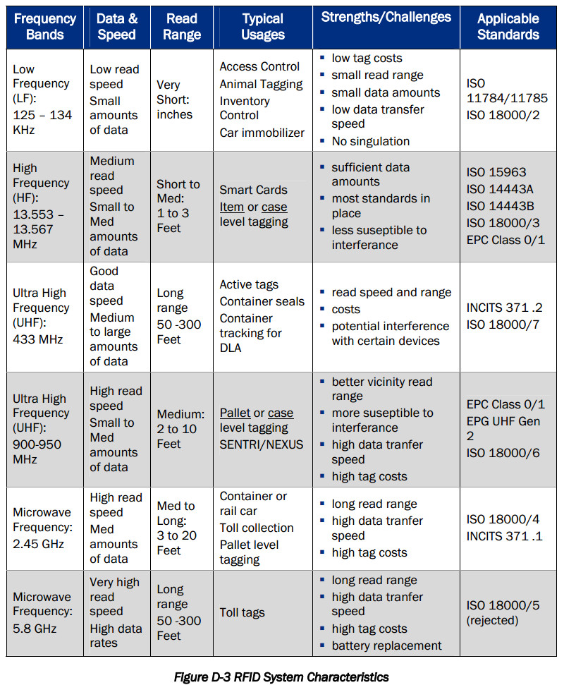
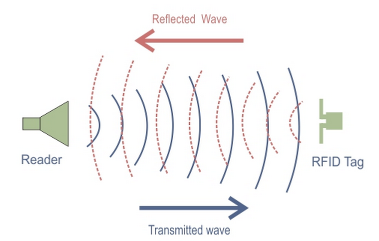
Frequency refers to the size of the radio waves used to communicate between RFID system components.
RFID systems throughout the world operate in low frequency (LF), high frequency (HF) and ultra-high frequency (UHF) bands.
Radio waves behave differently at each of these frequencies with advantages and disadvantages associated with using each frequency band.
If an RFID system operates at a lower frequency, it has a shorter read range and slower data read rate,
but increased capabilities for reading near or on metal or liquid surfaces.
If a system operates at a higher frequency, it generally has faster data transfer rates and longer read ranges than lower frequency systems,
but more sensitivity to radio wave interference caused by liquids and metals in the environment.
LF RFID
The LF band covers frequencies from 30 KHz to 300 KHz.
Typically LF RFID systems operate at 125 KHz, although there are some that operate at 134 KHz.
This frequency band provides a short read range of 10 cm, and has slower read speed than the higher frequencies,
but is not very sensitive to radio wave interference.
LF RFID applications include access control and livestock tracking.
Standards for LF animal-tracking systems are defined in ISO 14223, and ISO/IEC 18000-2.
The LF spectrum is not considered a truly global application because of slight differences in frequency and power levels throughout the world.
HF RFID
The HF band ranges from 3 to 30 MHz. Most HF RFID systems operate at 13.56 MHz with read ranges between 10 cm and 1 m.
HF systems experience moderate sensitivity to interference.
HF RFID is commonly used for ticketing, payment, and data transfer applications.
There are several HF RFID standards in place, such as the ISO 15693 standard for tracking items,
and the ECMA-340 and ISO/IEC 18092 standards for Near Field Communication (NFC),
a shortrange technology that is commonly used for data exchange between devices.
Other HF standards include the ISO/IEC 14443 A and ISO/IEC 14443 standards for MIFARE technology,
which used in smart cards and proximity cards,
and the JIS X 6319-4 for FeliCa, which is a smart card system commonly used in electronic money cards.
UHF RFID
The UHF frequency band covers the range from 300 MHz to 3 GHz.
Systems complying with the UHF Gen2 standard for RFID use the 860 to 960 MHz band.
While there is some variance in frequency from region to region,
UHF Gen2 RFID systems in most countries operate between 900 and 915 MHz.
The read range of passive UHF systems can be as long as 12 m, and UHF RFID has a faster data transfer rate than LF or HF.
UHF RFID is the most sensitive to interference, but many UHF product manufacturers have found ways of designing tags,
antennas, and readers to keep performance high even in difficult environments.
Passive UHF tags are easier and cheaper to manufacture than LF and HF tags.
UHF RFID is used in a wide variety of applications, ranging from retail inventory management,
to pharmaceutical anti-counterfeiting, to wireless device configuration.
The bulk of new RFID projects are using UHF opposed to LF or HF, making UHF the fastest growing segment of the RFID market.
The UHF frequency band is regulated by a single global standard called the ECPglobal Gen2 (ISO 18000-6C) UHF standard.

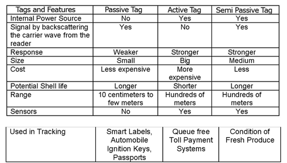
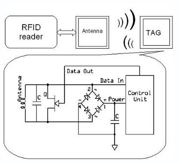
RFID is so called Radio Frequency Identification system which consists of two main parts:
transmitter and receiver.
The labels, access cards and even passports in some countries they have RFID transponders integrated.
There can be three types of RFID transponders:
Passive, Active and semi-passive.
Tags are grouped into three basic types:
- Passive: Passive RFID tags are by far the most common.
They do not contain any power and receive their operating power wirelessly from the RFID reader.
The amount of power is sufficient to power any component in the tag and reply with the required data.
The so-called RFID smart tags (or RFID smart labels) are all passive.
Furthermore, the tags use an antenna to capture energy from an RF signal emitted by the reader/writer. - Semi-passive: This form of tag contains a battery to supply power for the internal operation of the tag,
but relies on the RFID reader to supply the power to transmit the signal to the reader. - Active: An active tag is one in which battery power is used to supply power to the electronic circuits in the tag.
This extends the range of the tag and removes the dependency of the tag on received power to provide a reflected signal.
This also allows the control and processing circuits in the tag to be more sophisticated, as in the case of the semi-passive RFID tag.

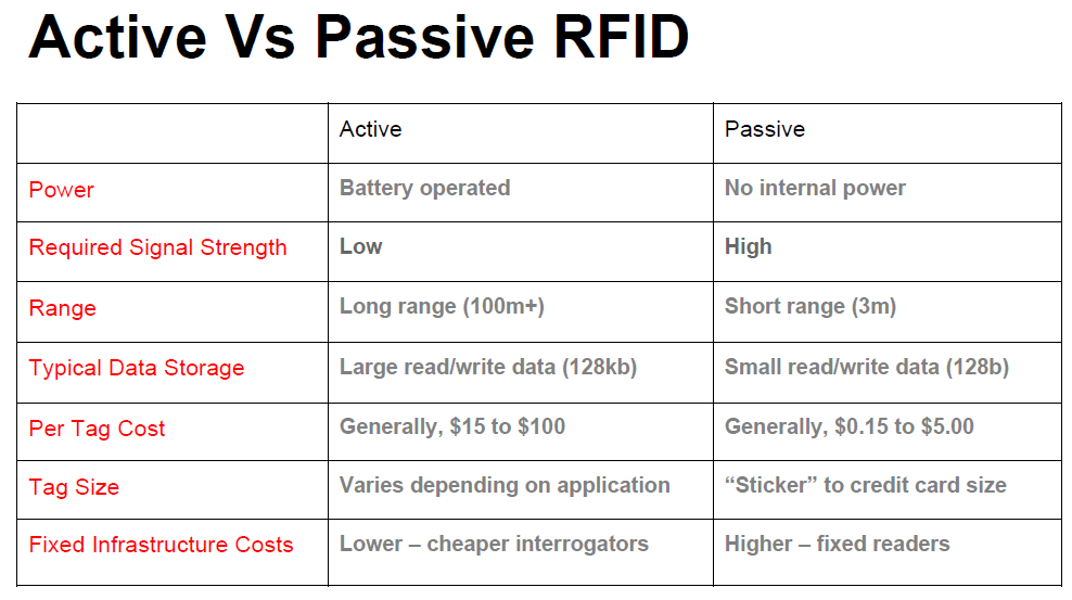
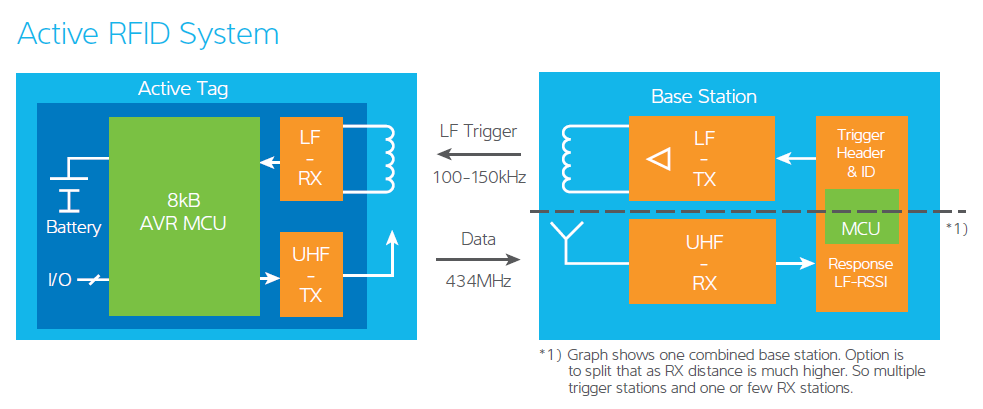
Passive, Active, and BAP RFID Systems
Active RFID Systems
In active RFID systems, tags have their own transmitter and power source.
Usually, the power source is a battery.
Active tags broadcast their own signal to transmit the information stored on their microchips.
Active RFID systems typically operate in the ultra-high frequency (UHF) band and offer a range of up to 100 m.
In general, active tags are used on large objects, such as rail cars, big reusable containers,
and other assets that need to be tracked over long distances.
There are two main types of active tags: transponders and beacons.
Transponders are “woken up” when they receive a radio signal from a reader,
and then power on and respond by transmitting a signal back.
Because transponders do not actively radiate radio waves until they receive a reader signal, they conserve battery life.
Beacons are used in most real-time locating systems (RTLS), in order to track the precise location of an asset continuously.
Unlike transponders, beacons are not powered on by the reader’s signal.
Instead, they emit signals at pre-set intervals. Depending on the level of locating accuracy required,
beacons can be set to emit signals every few seconds, or once a day.
Each beacon’s signal is received by reader antennas that are positioned around the perimeter of the area being monitored,
and communicates the tag’s ID information and position.
Passive RFID Systems
In passive RFID systems, the reader and reader antenna send a radio signal to the tag.
The RFID tag then uses the transmitted signal to power on, and reflect energy back to the reader.
Passive RFID systems can operate in the low frequency (LF), high frequency (HF) or ultra-high frequency (UHF) radio bands.
As passive system ranges are limited by the power of the tag’s backscatter
(the radio signal reflected from the tag back to the reader),they are typically less than 10 m.
Because passive tags do not require a power source or transmitter, and only require a tag chip and antenna,
they are cheaper, smaller, and easier to manufacture than active tags.
Passive tags can be packaged in many different ways, depending on the specific RFID application requirements.
For instance, they may be mounted on a substrate, or sandwiched between an adhesive layer and a paper label to create smart RFID labels.
Passive tags may also be embedded in a variety of devices or packages to make the tag resistant to extreme temperatures or harsh chemicals.
Passive RFID solutions are useful for many applications, and are commonly deployed to track goods in the supply chain,
to inventory assets in the retail industry, to authenticate products such as pharmaceuticals, and to embed RFID capability in a variety of devices.
Passive RFID can even be used in warehouses and distribution centers,
in spite of its shorter range, by setting up readers at choke points to monitor asset movement.
Battery-Assisted Passive (BAP) Systems
A Battery-Assisted Passive RFID tag is a type of passive tag which incorporates a crucial active tag feature.
While most passive RFID tags use the energy from the RFID reader’s signal to power on the tag’s chip and backscatter to the reader,
BAP tags use an integrated power source (usually a battery) to power on the chip,
so all of the captured energy from the reader can be used for backscatter.
Unlike transponders, BAP tags do not have their own transmitters.
Passive RFID tags

Transponders (tags) of passive RFID system don’t have power supply.
This is why they are called passive.
Passive tags are powered from electromagnetic field generated by reader antenna.
Reader antenna has to transmit enough power to provide enough energy to tag so it could to transmit back data.
Because of this reading distance is very limited – up to several centimeters.
Passive RFID tags do not have internal power supply.
Instead, they are powered by energy induced in the antenna by the RF signal.
Most passive tags transmit by backscattering the carrier signal from the reader.
The engineering challenge is to design an antenna that can collect power from the incoming signal
and transmit it to the outbound backscatter signal.
The response of a passive RFID tag is not necessarily just an ID number;
the tag chip can contain non-volatile EEPROM for storing data.


RFID Block Schematic

A simplified block schematic of an RFID tag (also called transponder) is shown in the diagram below.
Various components of the tag are as shown.
Normally, the antenna is external to the tag chip, and large in size.
The operation of the RFID tag is described below:
Handshaking with the Reader (interrogator):
- The reader continuously emits RF carrier signals, and keeps observing the received RF signals for data.
- The presence of a tag (for our discussion, we consider only passive tag) modulates the rf field, and the same is detected by the reader.
- The passive tag absorbs a small portion of the energy emitted by the reader,
and starts sending modulated information when sufficient energy is acquired from the rf field generated by the reader.
Note that the data modulation (modulation for 0s and 1s) is accomplished
by either direct modulation or FSK or Phase modulation. - The reader demodulates the signals received from the tag antenna, and decodes the same for further processing.
Well some of implementations may reach several meters.
Passive tags are most common used because they are cheap,
can last indefinitely long as there is no need for power supply,
and they are small size what allows them easy to integrate almost
in every environment starting wrists, necklaces, cards, stickers.
Passive tags simply consist of single IC and antena coil which is usually flat.
Passive tags are operating below 100MHz frequencies
(most common frequencies are 125kHz – 134.2kHz and 13.56MHz)
and main transfer energy is carried by magnetic field.
Magnetic field generated voltage in the coil which is used as power supply also as data signal.
There are also HF passive tags that operate at 900MHz and 2.45GHz.
These tags have dipole antena (1/8 wave length)construction.
With these tags distance may reach more than 3 meters.
But high frequency tags require more expensive manufacturing processing with more precise electronics,
but they can support up to 2Mb/s data stream.
Active RFID tags
Active RFID tags may provide all advantages of RFID system because tags are fully powered transmitters.
They don’t have to be activated by antenna reader.
Active RFID topic may be very wide because there are many areas where an how they can be used.
In some cases tags may not need a reader antena because tags in some particular cases can be configured to interact with each other.
Active transponders can communicate in very long ranges up to several hundred kilometers.
Main disadvantages of active tags may be relatively big size and production price compared to passive ones.

Semi-Passive RFID tags
Semi-Passive tags are more similar to passive transponders than active.
These tags are powered from battery or so called battery assisted tags,
but radio transmission depends on antena activity.
As data processor had it own power, so all received power can be used for transmitting back the signal
which is stronger than passive transducer.
This allows to increase communication distance with quit cheap solution.
Semi passive RFID tags augment the energy from reader antenna,
but they are not constantly beaming signals as active tags does.
Semi-passive RFID tags use a process to generate a tag response similar to that of passive tags.
Semi-passive tags differ from passive in that semi passive tags possess an internal battery
for the tag’s circuitry which allows the tag to complete other functions such as monitoring
of environmental conditions (temperature, shock) and which may extend the tag signal range.

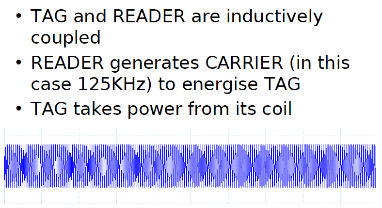
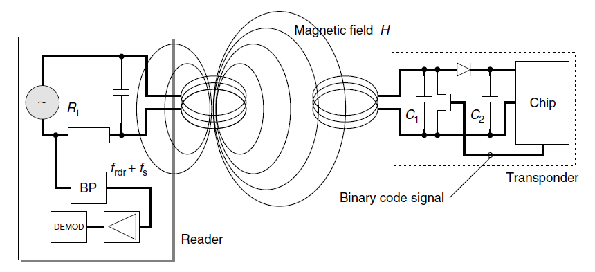
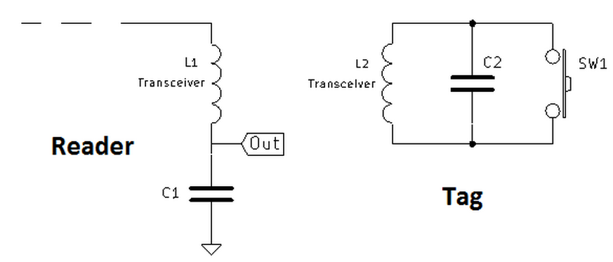
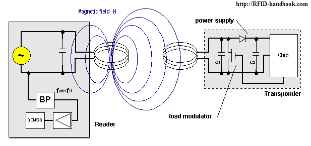
Power supply to an inductively coupled transponder from the energy of the magnetic alternating field generated by the reader
Signal transmission
Sound is converted into electricity by a telephone and then transmitted as an analog signal.
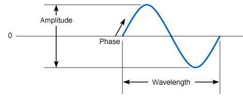
These waves have 3 fundamental characteristics:
- Amplitude, meaning the height (intensity) of the wave
- Frequency, which is the number of waves that pass in a single second and is measured in Hertz (cycles/second)
(wavelength, the length of the wave from crest to crest, is related to frequency.). - Phase is a third characteristic that describes the point in the wave’s cycle at which a wave begins and is measured in degrees.
(For example, changing a wave’s cycle from crest to trough corresponds to a 180 degree phase shift).
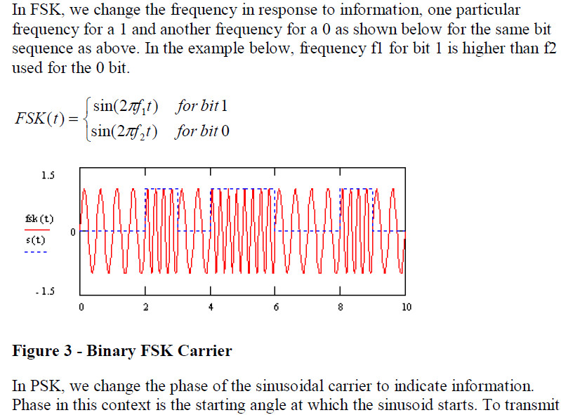
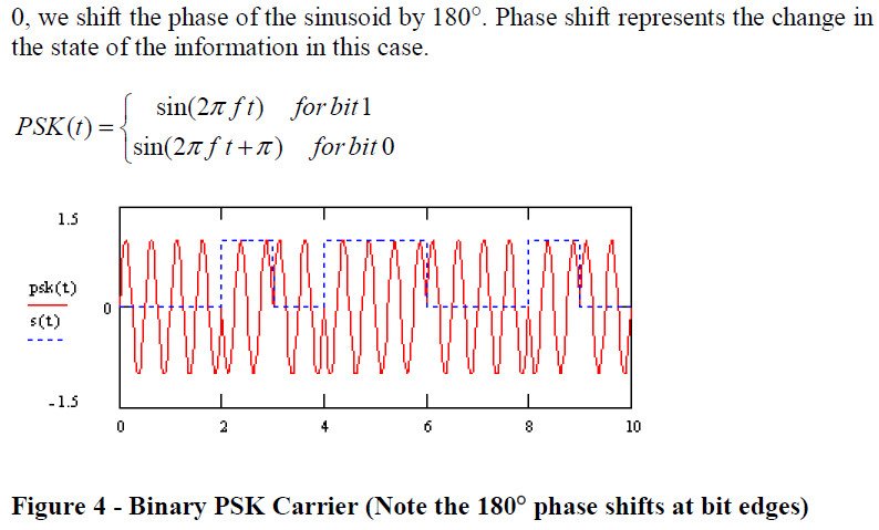
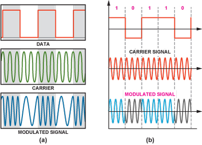
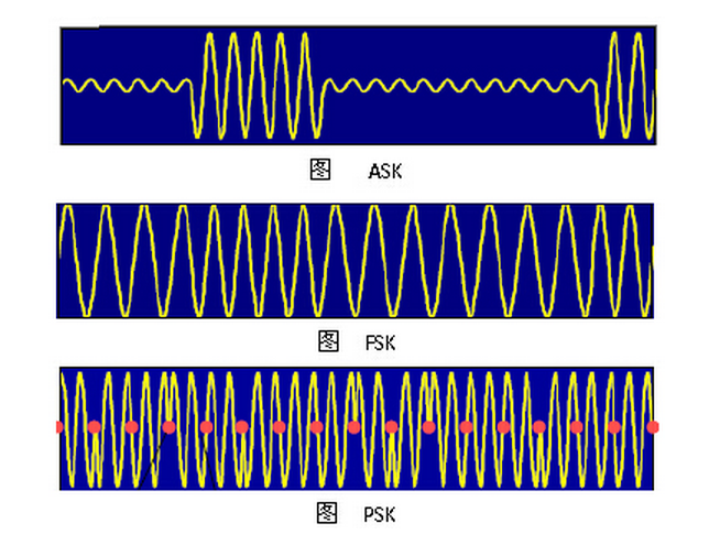
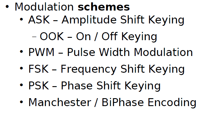
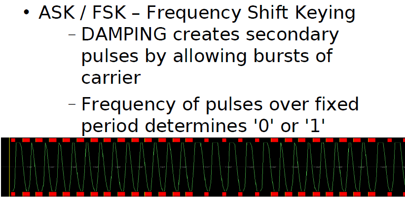
Most RFID tags were using ASK (Amplitude Shift Keying), FSK (Frequency Shift Keying) and PSK (Phase Shift Keying) for its analog modulation.

All known digital modulation procedures are used in data transfer from the reader to the transponder
in full and half duplex systems, irrespective of the operating frequency or the coupling procedure.
There are three basic procedures:
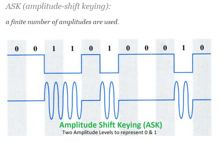
- ASK: amplitude shift keying
- FSK: frequency shift keying
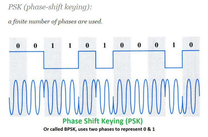
- PSK: phase shift keying
- ASK ——幅移鍵控調製,把二進位制符號0和1分別用不同的幅度來表示。
- FSK ——頻移鍵控調製,即用不同的頻率來表示不同的符號。
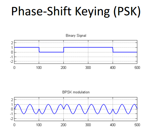
- PSK ——相移鍵控調製,通過二進位制符號0和1來判斷訊號前後相位。
Because of the simplicity of demodulation, the majority of systems use ASK modulation
Modulation is the process process of modifying modifying the characteristics of a signal,
called a carrier wave, to convey information information.
The characteristics of a signal to modify include amplitude, frequency frequency, and phase.
http://electronicdesign.com/communications/understanding-modern-digital-modulation-techniques
Fundamental to all wireless communications is modulation, the process of impressing the data to be transmitted on the radio carrier. Most wireless transmissions today are digital, and with the limited spectrum available, the type of modulation is more critical than it has ever been.
The main goal of modulation today is to squeeze as much data into the least amount of spectrum possible. That objective, known as spectral efficiency, measures how quickly data can be transmitted in an assigned bandwidth. The unit of measurement is bits per second per Hz (b/s/Hz). Multiple techniques have emerged to achieve and improve spectral efficiency.
Table of Contents
- Amplitude Shift Keying (ASK) and Frequency Shift Keying (FSK)
- Binary Phase Shift Keying (BPSK) and Quadrature Phase Shift Keying (QPSK)
- Data Rate And Baud Rate
- Multiple Phase Shift Keying (M-PSK)
- Quadrature Amplitude Modulation (QAM)
- Amplitude Phase Shift Keying (APSK)
- Orthogonal Frequency Division Multiplexing
- Determining Spectral Efficiency
- Other Factors Affecting Spectral Efficiency
- Implementing Modulation And Demodulation
- The Pursuit Of Greater Spectral Efficiency
- Acknowledgment
- References
Amplitude Shift Keying (ASK) and Frequency Shift Keying (FSK)
There are three basic ways to modulate a sine wave radio carrier:
modifying the amplitude, frequency, or phase.
More sophisticated methods combine two or more of these variations to improve spectral efficiency.
These basic modulation forms are still used today with digital signals.
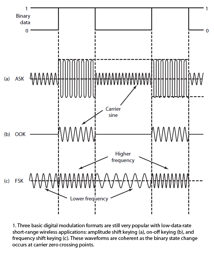
Figure 1 shows a basic serial digital signal of binary zeros and ones to be transmitted and the corresponding AM and FM signals resulting from modulation.
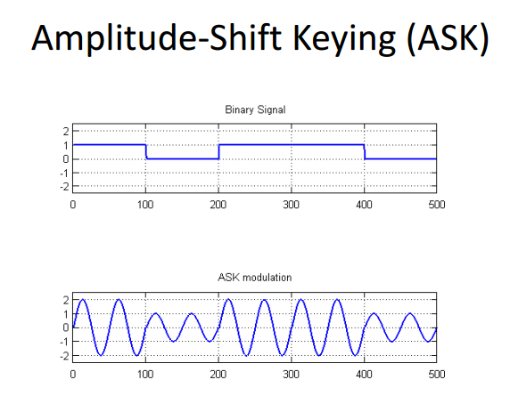
There are two types of AM signals: on-off keying (OOK) and amplitude shift keying (ASK).
In Figure 1a, the carrier amplitude is shifted between two amplitude levels to produce ASK.
InFigure 1b, the binary signal turns the carrier off and on to create OOK.
AM produces sidebands above and below the carrier equal to the highest frequency content of the modulating signal.
The bandwidth required is two times the highest frequency content including any harmonics for binary pulse modulating signals.
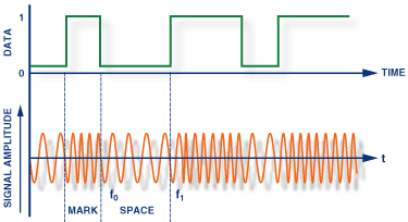
Frequency shift keying (FSK) shifts the carrier between two different frequencies called the mark and space frequencies, or fm and fs(Fig. 1c).
FM produces multiple sideband frequencies above and below the carrier frequency.
The bandwidth produced is a function of the highest modulating frequency including harmonics and the modulation index, which is:
m = Δf(T)
Δf is the frequency deviation or shift between the mark and space frequencies, or:
Δf = fs – fm
T is the bit time interval of the data or the reciprocal of the data rate (1/bit/s).
Smaller values of m produce fewer sidebands.
A popular version of FSK called minimum shift keying (MSK) specifies m = 0.5. Smaller values are also used such as m = 0.3.
Here are two ways to further improve the spectral efficiency for both ASK and FSK.
First, select data rates, carrier frequencies, and shift frequencies so there are no discontinuities in the sine carrier when changing from one binary state to another.
These discontinuities produce glitches that increase the harmonic content and the bandwidth.
The idea is to synchronize the stop and start times of the binary data with when the sine carrier is transitioning in amplitude or frequency at the zero crossing points.
This is called continuous phase or coherent operation. Both coherent ASK/OOK and coherent FSK have fewer harmonics and a narrower bandwidth than non-coherent signals.
A second technique is to filter the binary data prior to modulation. This rounds the signal off, lengthening the rise and fall times and reducing the harmonic content.
Special Gaussian and raised cosine low pass filters are used for this purpose. GSM cell phones widely use a popular combination, Gaussian filtered MSK (GMSK),
which allows a data rate of 270 kbits/s in a 200-kHz channel.
Binary Phase Shift Keying (BPSK) And Quadrature Phase Shift Keying (QPSK)
A very popular digital modulation scheme, binary phase shift keying (BPSK), shifts the carrier sine wave 180° for each change in binary state (Fig. 2).
BPSK is coherent as the phase transitions occur at the zero crossing points.
The proper demodulation of BPSK requires the signal to be compared to a sine carrier of the same phase. This involves carrier recovery and other complex circuitry.
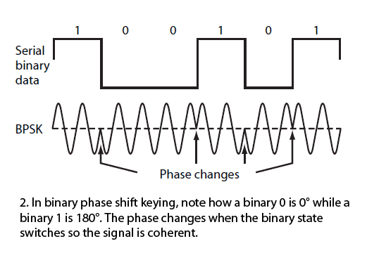
2. In binary phase shift keying, note how a binary 0 is 0° while a binary 1 is 180°.
The phase changes when the binary state switches so the signal is coherent.
A simpler version is differential BPSK or DPSK, where the received bit phase is compared to the phase of the previous bit signal.
BPSK is very spectrally efficient in that you can transmit at a data rate equal to the bandwidth or 1 bit/Hz.
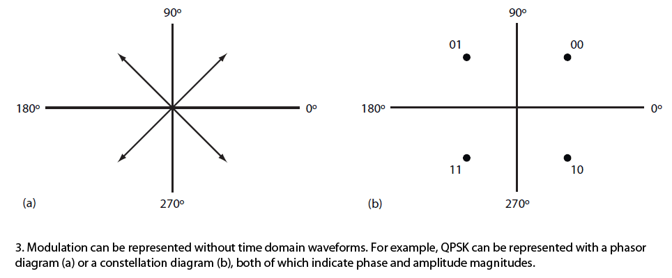
In a popular variation of BPSK, quadrature PSK (QPSK), the modulator produces two sine carriers 90° apart.
The binary data modulates each phase, producing four unique sine signals shifted by 45° from one another.
The two phases are added together to produce the final signal. Each unique pair of bits generates a carrier with a different phase (Table 1).
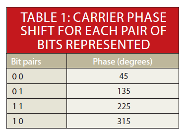
Figure 3a illustrates QPSK with a phasor diagram where the phasor represents the carrier sine amplitude peak and its position indicates the phase.
A constellation diagram in Figure 3b shows the same information.
QPSK is very spectrally efficient since each carrier phase represents two bits of data.
The spectral efficiency is 2 bits/Hz, meaning twice the data rate can be achieved in the same bandwidth as BPSK.
Data Rate And Baud Rate
The maximum theoretical data rate or channel capacity (C) in bits/s is a function of the channel bandwidth (B) channel in Hz and the signal-to-noise ratio (SNR):
C = B log2 (1 + SNR)
This is called the Shannon-Hartley law. The maximum data rate is directly proportional to the bandwidth and logarithmically proportional the SNR.
Noise greatly diminishes the data rate for a given bit error rate (BER).
Another key factor is the baud rate, or the number of modulation symbols transmitted per second.
The term symbol in modulation refers to one specific state of a sine carrier signal.
It can be an amplitude, a frequency, a phase, or some combination of them. Basic binary transmission uses one bit per symbol.
In ASK, a binary 0 is one amplitude and a binary 1 is another amplitude.
In FSK, a binary 0 is one carrier frequency and a binary 1 is another frequency.
BPSK uses a 0° shift for a binary 0 and a 180° shift for a binary 1.
In each of these cases there is one bit per symbol.
Data rate in bits/s is calculated as the reciprocal of the bit time (tb):
bits/s = 1/tb
With one symbol per bit, the baud rate is the same as the bit rate.
However, if you transmit more bits per symbol, the baud rate is slower than the bit rate by a factor equal to the number of bits per symbol.
For example, if 2 bits per symbol are transmitted, the baud rate is the bit rate divided by 2.
For instance, with QPSK a 70 Mb/s data stream is transmitted at a baud rate of 35 symbols/second.
Multiple Phase Shift Keying (M-PSK)
QPSK produces two bits per symbol, making it very spectrally efficient. QPSK can be referred to as 4-PSK because there are four amplitude-phase combinations. By using smaller phase shifts, more bits can be transmitted per symbol. Some popular variations are 8-PSK and 16-PSK.
8-PSK uses eight symbols with constant carrier amplitude 45° shifts between them, enabling three bits to be transmitted for each symbol. 16-PSK uses 22.5° shifts of constant amplitude carrier signals. This arrangement results in a transmission of 4 bits per symbol.
While Multiple Phase Shift Keying (M-PSK) is much more spectrally efficient, the greater the number of smaller phase shifts, the more difficult the signal is to demodulate in the presence of noise. The benefit of M-PSK is that the constant carrier amplitude means that more efficient nonlinear power amplification can be used.
Quadrature Amplitude Modulation (QAM)
The creation of symbols that are some combination of amplitude and phase can carry the concept of transmitting more bits per symbol further.
This method is called quadrature amplitude modulation (QAM).
For example, 8QAM uses four carrier phases plus two amplitude levels to transmit 3 bits per symbol.
Other popular variations are 16QAM, 64QAM, and 256QAM, which transmit 4, 6, and 8 bits per symbol respectively(Fig. 4).
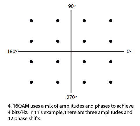
While QAM is enormously efficient of spectrum, it is more difficult to demodulate in the presence of noise, which is mostly random amplitude variations.
Linear power amplification is also required. QAM is very widely used in cable TV, Wi-Fi wireless local-area networks (LANs), satellites, and cellular telephone systems
to produce maximum data rate in limited bandwidths.
Amplitude Phase Shift Keying (APSK)
Amplitude phase shift keying (APSK), a variation of both M-PSK and QAM, was created in response to the need for an improved QAM.
Higher levels of QAM such as 16QAM and above have many different amplitude levels as well as phase shifts. These amplitude levels are more susceptible to noise.
Furthermore, these multiple levels require linear power amplifiers (PAs) that are less efficient than nonlinear (e.g., class C).
The fewer the number of amplitude levels or the smaller the difference between the amplitude levels, the greater the chance to operate in the nonlinear region of the PA to boost power level.
APSK uses fewer amplitude levels. It essentially arranges the symbols into two or more concentric rings with a constant phase offset θ.
For example, 16APSK uses a double-ring PSK format (Fig. 5). This is called 4-12 16APSK with four symbols in the center ring and 12 in the outer ring.
Two close amplitude levels allow the amplifier to operate closer to the nonlinear region, improving efficiency as well as power output.
APSK is used primarily in satellites since it is a good fit with the popular traveling wave tube (TWT) PAs.
Orthogonal Frequency Division Multiplexing (OFDM)
Orthogonal frequency division multiplexing (OFDM) combines modulation and multiplexing techniques to improve spectral efficiency.
A transmission channel is divided into many smaller subchannels or subcarriers. The subcarrier frequencies and spacings are chosen so they’re orthogonal to one another.
Their spectra won’t interfere with one another, then, so no guard bands are required (Fig. 6).
The serial digital data to be transmitted is subdivided into parallel slower data rate channels. These lower data rate signals are then used to modulate each subcarrier.
The most common forms of modulation are BPSK, QPSK, and several levels of QAM. BPSK, QPSK, 16QAM, and 64QAM are defined with 802.11n.
Data rates up to about 300 Mbits/s are possible with 64QAM.
The complex modulation process is only produced by digital signal processing (DSP) techniques.
An inverse fast Fourier transform (IFFT) generates the signal to be transmitted. An FFT process recovers the signal at the receiver.
OFDM is very spectrally efficient. That efficiency level depends on the number of subcarriers and the type of modulation, but it can be as high as 30 bits/s/Hz.
Because of the wide bandwidth it usually occupies and the large number of subcarriers, it also is less prone to signal loss due to fading, multipath reflections,
and similar effects common in UHF and microwave radio signal propagation.
Currently, OFDM is the most popular form of digital modulation.
It is used in Wi-Fi LANs, WiMAX broadband wireless, Long Term Evolution (LTE) 4G cellular systems, digital subscriber line (DSL) systems,
and in most power-line communications (PLC) applications. For more, see “Orthogonal Frequency-Division Multiplexing (OFDM): FAQ Tutorial.”
Determining Spectral Efficiency
Again, spectral efficiency is a measure of how quickly data can be transmitted in an assigned bandwidth, and the unit of measurement is bits/s/Hz (b/s/Hz).
Each type of modulation has a maximum theoretical spectral efficiency measure (Table 2).
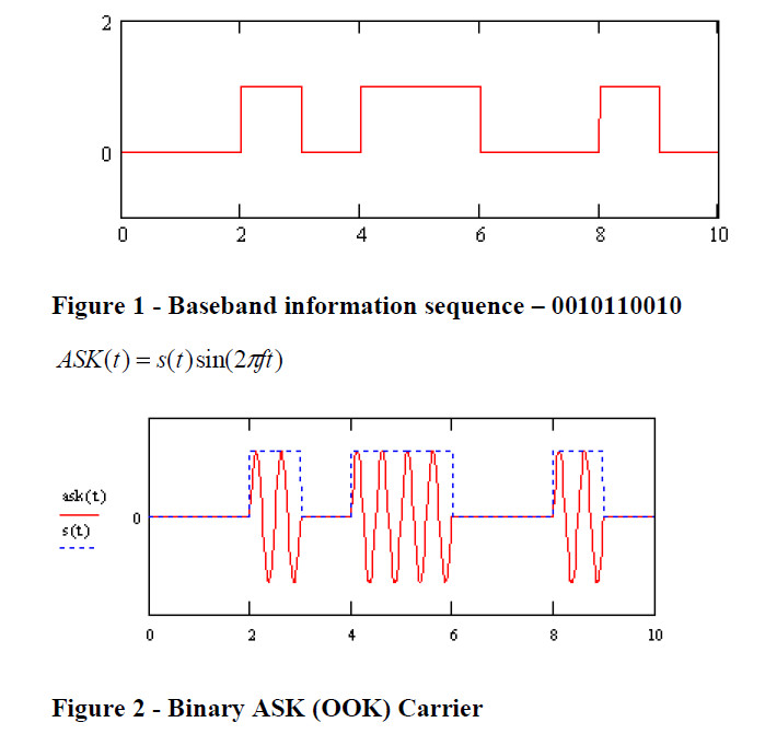
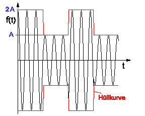
ASK是幅移鍵控調製的簡寫,例如二進位制的,把二進位制符號0和1分別用不同的幅度來表示,就是ASK了。 而
OOK則是ASK調製的一個特例,把一個幅度取為0,另一個幅度為非0,就是OOK了。例如二進位制符號0用不發射載波表示,二進位制1用發射1表示。
ASK跟OOK的頻譜都比較寬。
FSK是頻移鍵控調製的簡寫,即用不同的頻率來表示不同的符號。例如2KHz表示符號0,3KHz表示符號1。
GFSK是高斯頻移鍵控的簡寫,在調製之前通過一個高斯低通濾波器來限制訊號的頻譜寬度。
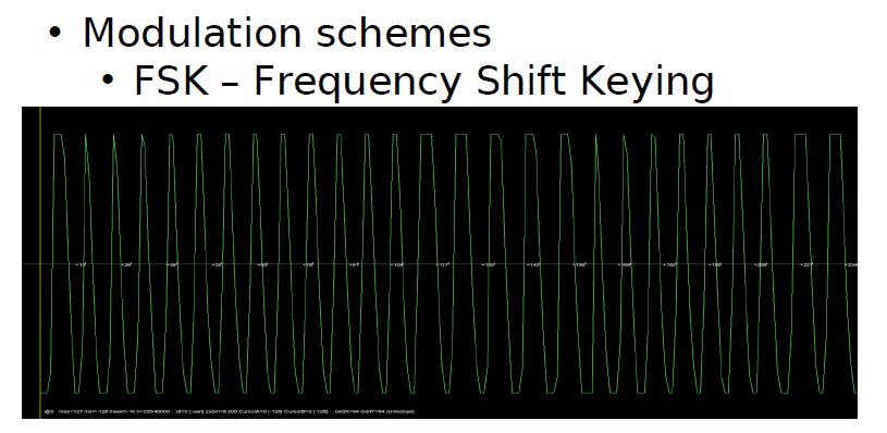
FSK(Frequency-shift keying):頻移鍵控。就是用數字訊號去調製載波的頻率。是資訊傳輸中使用得較早的一種調製方式,它的主要優點是:
實現起來較容易,抗噪聲與抗衰減的效能較好。在中低速資料傳輸中得到了廣泛的應用。
ASK: 幅移鍵控ASK (Amplitude Shift Keying)
ASK指的是振幅鍵控方式。這種調製方式是根據訊號的不同,調節正弦波的幅度。
幅度鍵控可以通過乘法器和開關電路來實現。載波在數字訊號1或0的控制下通或斷,在訊號為1的狀態載波接通,此時傳輸通道上有載波出現;
在訊號為0的狀態下,載波被關斷,此時傳輸通道上無載波傳送。那麼在接收端我們就可以根據載波的有無還原出數字訊號的1和0。
對於二進位制幅度鍵控訊號的頻頻寬度為二進位制基帶訊號寬度的兩倍。
幅移鍵控法(ASK)的載波幅度是隨著調製訊號而變化的, 其最簡單的形式是,載波在二進位制調製訊號控制下通斷, 此時又可稱作開關鍵控法(OOK)。
多電平MASK調製方式是一種比較高效的傳輸方式,但由於它的抗噪聲能力較差,尤其是抗衰落的能力不強,因而一般只適宜在恆參通道下采用。
ASK定義
“移幅鍵控”又稱為“振幅鍵控”(Amplitude Shift Keying),記為ASK,是調製技術的一種常用方式。
如果數字調製訊號的可能狀態與二進位制資訊符號或它的相應基帶訊號狀態一一對應,則稱其已調訊號為二進位制數字調製訊號。
用二進位制資訊符號進行鍵控,稱為二進位制振幅鍵控,用2ASK表示。
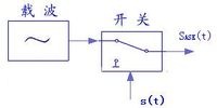
圖1:移幅鍵控原理圖
在“移幅鍵控”方式中,當“1”出現時接通振幅為A的載波,“0”出現時關斷載波,這相當於將原基帶訊號(脈衝列)頻譜搬到了載波的兩側。
移幅鍵控(ASK)相當於模擬訊號中的調幅,只不過與載頻訊號相乘的是二進位制數碼而已。
移幅就是把頻率、相位作為常量,而把振幅作為變數,資訊位元是通過載波的幅度來傳遞的。
二進位制振幅鍵控(2ASK),由於調製訊號只有0或1兩個電平,相乘的結果相當於將載頻或者關斷,或者接通,
它的實際意義是當調製的數字訊號為“1”時,傳輸載波;當調製的數字訊號為“0”時,不傳輸載波。
原理如圖1所示,其中s(t)為基帶矩形脈衝。一般載波訊號用餘弦訊號,而調製訊號是把數字序列轉換成單極性的基帶矩形脈衝序列,
而這個通斷鍵控的作用就是把這個輸出與載波相乘,就可以把頻譜搬移到載波頻率附近,實現2ASK。實現後的2ASK波形如圖2所示。
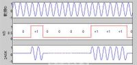
圖2:輸出後的2ASK波形
移幅鍵控這種調製技術工作的最簡單和最常用的形式是開關,載波存在用“1”代表,載波不存在用“0”代表。
這種型別的調製稱為開關鍵控(OOK),是最節省能量的調製方式,因為只有在傳送“1”時輻射能量。
幅移鍵控需要很高的訊雜比才能解調訊號,因為根據其本身特性,大部分訊號都是以很低的功率進行發射的。
ASK調製射頻系統的優點是發射和接收裝置的結構簡單,並且功耗比較低。
但不幸的是,ASK/OOK調製系統所佔用的頻寬低於500kHz或著峰值密度根本不會落入“數字調製系統”要求的範圍。
這表明ASK/OOK調製系統的發射功率被限制在50mV/m,或者必須採用一些FHSS技術以滿足FCC的15.247條款的要求。
OOK On-Off Keying
OOK是ASK調製的一個特例,把一個幅度取為0,另一個幅度為非0,就是OOK。
二進位制啟閉鍵控(OOK:On-Off Keying)又名二進位制振幅鍵控(2ASK),它是以單極性不歸零碼序列來控制正弦載波的開啟與關閉。
該調製方式的出現比模擬調製方式還早,Morse碼的無線電傳輸就是使用該調製方式。
由於OOK的抗噪聲效能不如其他調製方式,所以該調製方式在目前的衛星通訊、數字微波通訊中沒有被採用,
但是由於該調製方式的實現簡單,在光纖通訊系統中,振幅鍵控方式卻獲得廣泛應用。
該調製方式的分析方法是基本的,因而可從OOK調製方式入門來研究數字調製的基本理論。
FSK頻移鍵控
中文名稱:頻移鍵控
英文名稱:frequency-shift keying;
FSK 定義:
正弦振盪的頻率在一組離散值間改變的角度調製,其中每一離散值表示時間離散調製訊號的一種特徵狀態。
應用學科:通訊科技(一級學科);通訊原理與基本技術(二級學科)
頻移鍵控,英文縮寫FSK
頻移鍵控是利用兩個不同頻率F1和F2的振盪源來代表訊號1和0。
用數字訊號的1和0去控制兩個獨立的振盪源交替輸出。
對二進位制的頻移鍵控調製方式,其有效頻寬為B=2xF+2Fb,xF是二進位制基帶訊號的頻寬也是FSK訊號的最大頻偏,
由於數字訊號的頻寬即Fb值大,所以二進位制頻移鍵控的訊號頻寬比較大,頻帶利用率小。
Binary Keying
Binary Keying definition:
The bits in a message stream switch the modulation parameters (amplitude, freque ncy and phase) from one state to another.
This process is called binary keying.
Binary keying is a process that makes the values of amplitude, phase or frequency of the carrier signal change
in sympathy with the values of the bits in the binary signal tream.
Basic actions can be classified as:
– ASK – Amplitude Shift Keying
– PSK – Phase Shift Keying
– FSK – Frequency Shift Keying
- OOK - On-Off Keying is also known as Amplitude Shift Keying (ASK)
- BPSK - Binary or Bi-Phase Shift Keying
- QPSK - Quadrature Phase Shift Keying
- MSK - Minimum Shift Keying
- DPSK - Differential PSK
- 8PSK - 8 Phase Shift Keying
http://www.cse.iitk.ac.in/users/dheeraj/cs425/lec03.html
Digital data to analog signals
A modem (modulator-demodulator) converts digital data to analog signal. There are 3 ways to modulate a digital signal on an analog carrier signal.
Amplitude shift keying (ASK):
is a form of modulation which represents digital data as variations in the amplitude of a carrier wave.
Two different amplitudes of carrier frequency represent '0' , '1'.
Frequency shift keying (FSK):
In Frequency Shift Keying, the change in frequency define different digits. Two different frequencies near carrier frequency represent '0' ,''1'.
Phase shift keying (PSK):
The phase of the carrier is discretely varied in relation either to a reference phase or to the phase of the immediately preceding signal element,
in accordance with data being transmitted. Phase of carrier signal is shifted to represent '0' , '1'.

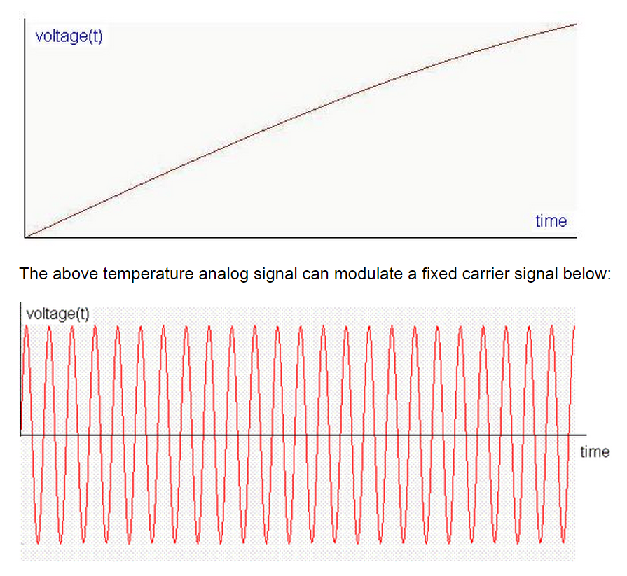
The origin of all radio modulation techniques stem back to the AM and FM basic modulation. AM modulation changes the carrier frequency according to the data signal while the FM changes the carrier frequency according to the data signal. The information signal varies with time such as it could increase, decrease, or vanish to zero. The following signal represents a temperature increase as function of time. The temperature starts from zero at the bottom left and increases as time goes by. This analog temperature signal is converted to a voltage signal voltage(t) where the voltage tracks temperature as function of time:
In AM modulation the carrier frequency is kept the same but the amplitude of the carrier is changed according to the temperature signal as follow:
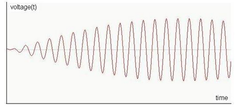
In FM modulation the amplitude of the carrier is kept the same but the carrier frequency is changed according to the temperature signal as follow:
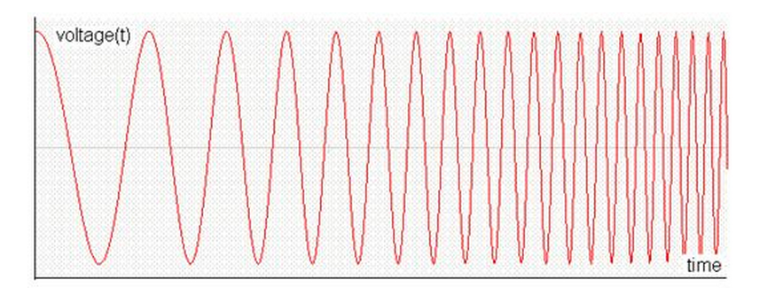
The temperature reading is then transmitted in form of radio signal and picked by the radio receiver. The receiver then extracts the information from the radio signal (AM or FM) by analyzing the variation in amplitude or frequency. The same rules of amplitude and frequency variations are followed when transmitting or receiving the data signal.
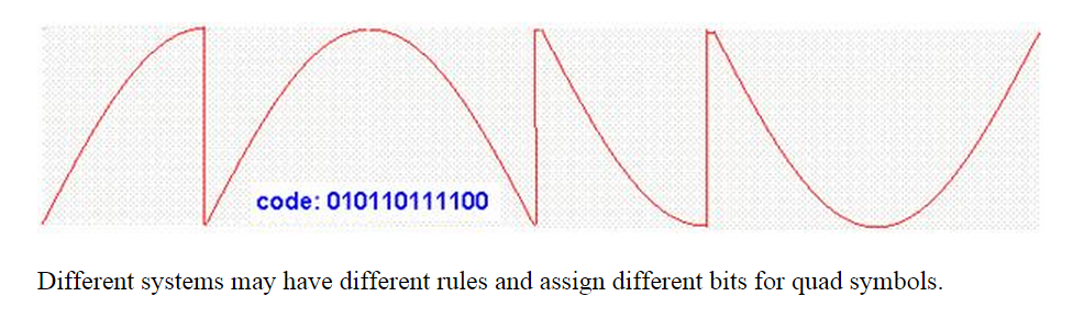
From the above methods of AM and FM modulations different forms of radio modulations are derived. The ON-OFF Keying (OOK) technique described above is a derived form of AM modulation. Frequency Hopping Spread Spectrum (FHSS) is an advanced form of FM modulation. Other modulation techniques such as Frequency Shift Keying (FSK), Phase Shift Keying (PSK), and In phase – Out of phase (IQ) modulation, Quadrate Phase Shift Keying (QPSK) modulation are also derived forms of FM modulation. The key is that the sine wave is divided into equal number of sections (4, 8, 16, 32) and the correct section is used to associate the data symbol to. Phase modulation and frequency modulation are related to one another and many rules equally apply to both of them. The sine wave can be divided into 4 quarters (Quad Modulation) each of the quad having 90 degrees. Here is how the sine wave is divided into 4 equal sections

Details of the sine wave quads are used to carry useful information in the radio waves. These quads are transmitted wirelessly in series from the transmitter to the receiver.The IQ modulation could be use for very high speed communication. Each quad is assigned for example two digital bits as follow:
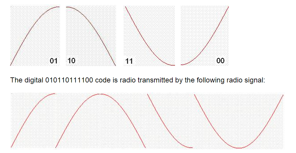
By doing so the power consumptions is minimized, communication speed is multiplied, but the possibility of transmit error is increased.
Here is how the above radio signal may look like using the oscilloscope:


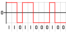
On-Off Keying (OOK)
Most current optical transmission systems encode the signal as a sequence of light pulses in a binary form.
This is called “on-off keying” (OOK).
Sometimes this is described as amplitude modulation, comparing it to AM radio.
In fact, the technique is nothing like AM radio.
An AM radio carries an analogue signal.
The amplitude of the carrier is continuously varied (modulated) in accordance with variations in the signal.
The receiver recovers the signal from the variations of the carrier.
But in an optical system, it is much more like a very simple form of digital baseband transmission in the electronic world.
The signal is there or it isn’t; beyond this the amplitude of the signal doesn’t matter.
In fairness, you can call OOK a special case of amplitude shift keying (ASK)
in which a number of discrete signal amplitude levels are used to carry a digital signal.
The signal power is kept large (m = 1) to indicate a binary '1'
and small or zero (m = 0) to represent a binary '0'.
An example is shown in Figure 3.6. In OOK, each symbol is a period of fixed duration
in which the signal power is either high or low.
Each OOK symbol represents one binary bit, though other types of symbols can convey more than one bit each.
Any circuit that can change the output power, such as a simple switch,can be used to create an OOK signal,
and any circuit that can detect power levels can demodulate (extract the data from) the signal.
For example, a diode (an electrical component that passes electrical current only in one direction
and blocks current flow in the opposite direction) can rectify a high-frequency signal, turning it into pulses of DC.
These pulses can be smoothed with a storage capacitor to produce an output signal that looks very much like the baseband signal m(t).
If the diode responds rapidly, it can be used at very high frequencies.
Modern diodes can operate up to over 1 GHz, allowing passive RFID tags to demodulate a reader signal using only a diode and capacitor.
Unmodified OOK is admirably simple and seems promising as a method of modulating a reader signal.


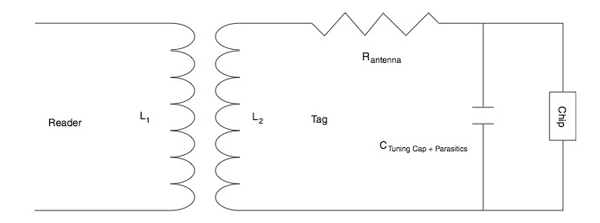
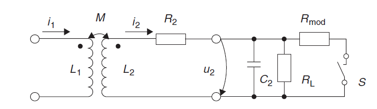
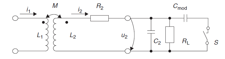
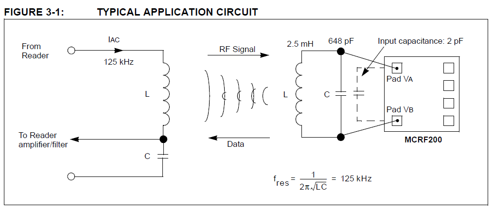
Because communications, power, communications, and synchronization flow through the antenna, antenna design is critical for successful RFID applications.
The typical parallel resonant circuit of a tag antenna comprises the inductance, resistance, and capacitance of the antenna loop (see Fig. 2)
with resonant frequency fres = 1/(2π√(L_2 C)).
In this equivalent circuit, the loop capacitance is the sum of the tuning capacitance and parasitic capacitances of the antenna coil and tag materials.
Antenna designers work to keep coil resistance to a minimum to increase the Q of the antenna and so maximize the energy available to the tag.
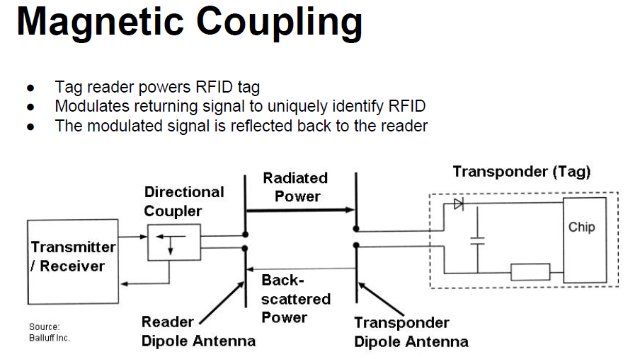
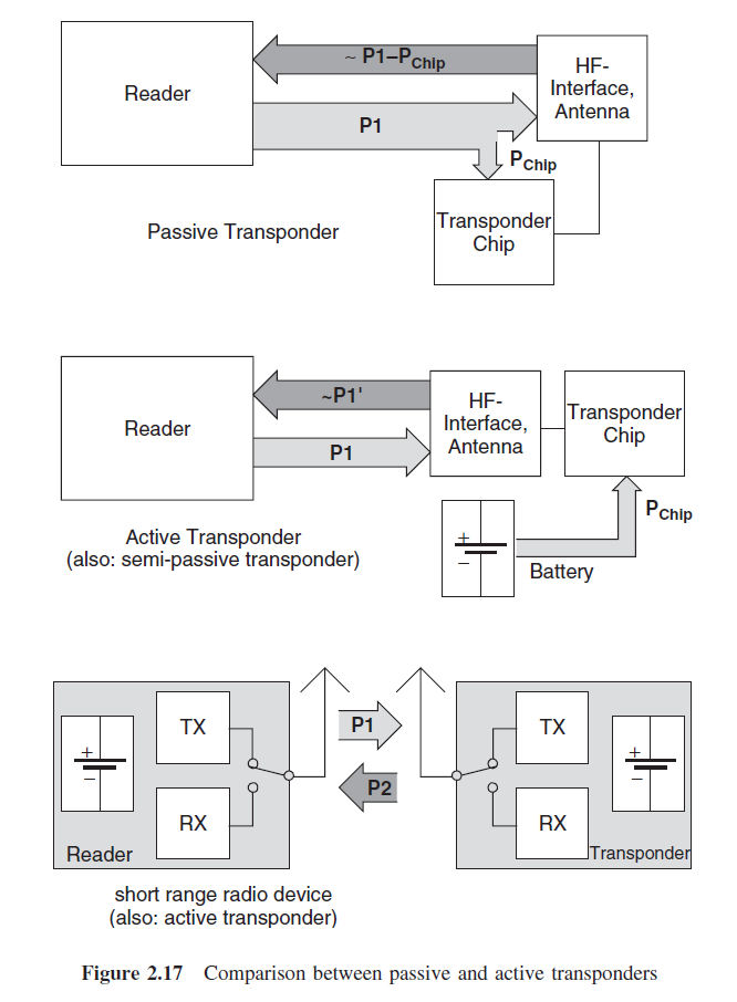
In passive RFID, the reader and tag antennas form a transformer,
so the RF signal transmitted by the reader energizes the parallel resonant circuit formed by the antenna coil and tag capacitance.
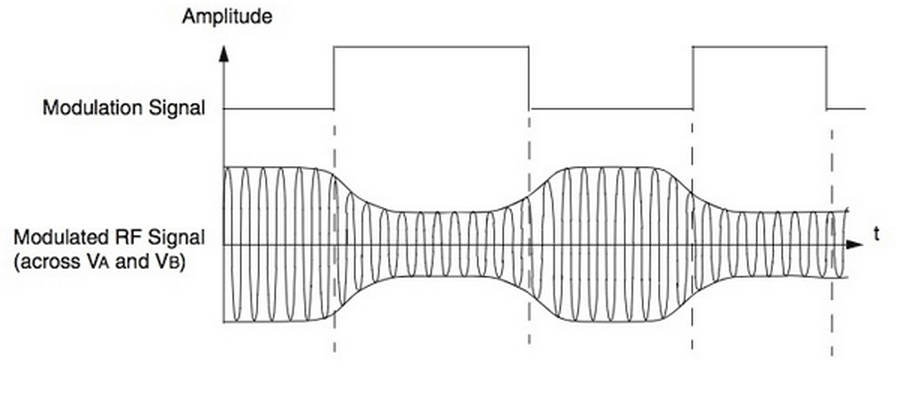
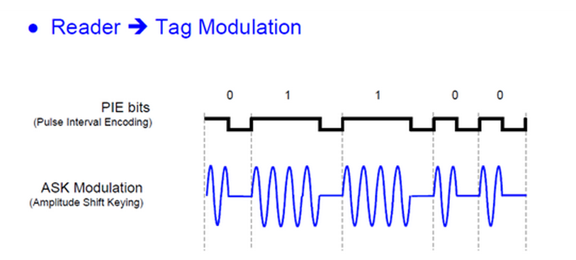
In passive RFID systems, readers communicate with tags by modulating the amplitude, phase, or frequency of the carrier,
according to the specific design of the RFID system.
Tags respond using methods that depend on whether the tag is operating in the near field or far field of the reader.
Near-field communications takes advantage of the inductive coupling of the reader and tag antennas.
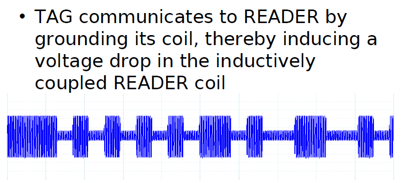
Here, the tag communicates its data by varying the load on its antenna coil,
which affects the voltage on the antenna — and signal seen by the reader.
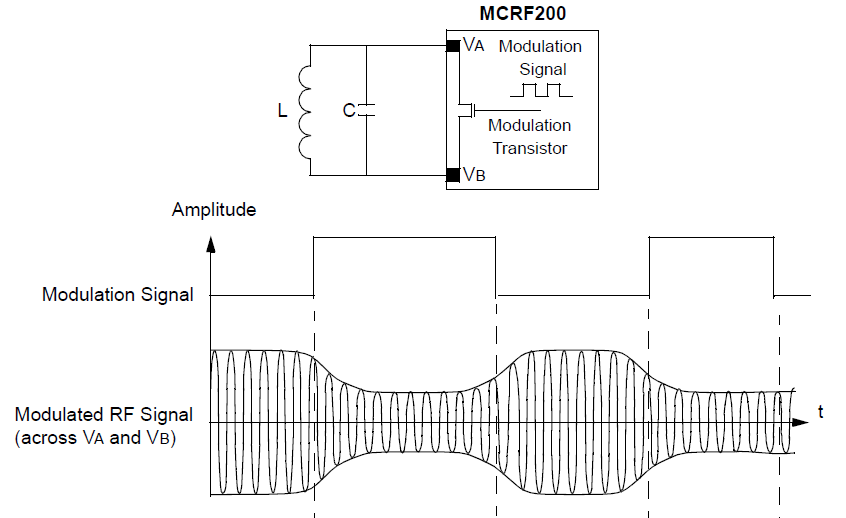
By switching the coil load on and off rapidly, the tag can communicate its response as a modulation of the RF carrier (see Fig. 3).
Diverse tag designs implement widely different variations of this basic amplitude shift keying (ASK)
approach to support communications using other modulation methods including frequency shift keying (FSK),
phase shift keying (PSK), pulse position modulation (PPM),
pulse duration modulation (PDM), and phase jitter modulation (PJM), among others.
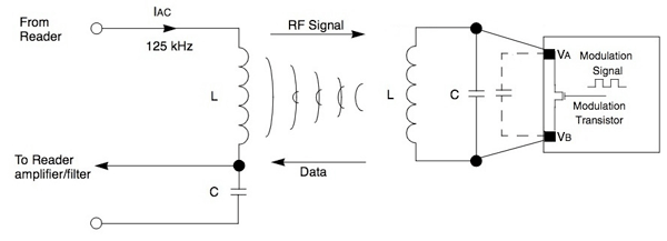
By driving a transistor with a modulating signal, a tag can vary the load on the antenna resonant circuit (a)
to transmit data as a modulated RF signal back to a reader.
In this example, a tag with a 2.5-mH loop antenna connected to its antenna pads (VA and VB)
would require a 648-pF capacitor (assuming 2-pF parasitic capacitance illustrated by a dashed line)
to resonant at the 125-kHz operating frequency.
Often, tag communication methods require peak power beyond that acquired through inductive coupling.
In these cases, the tag design typically includes an additional capacitor.
During a power phase of the communications protocol, the reader carrier energizes the resonant circuit in the tag as usual,
but now this induced voltage is rectified by the tag chip to charge the capacitor.
At the end of the power phase, the tag transmits its data using the energy stored in the capacitor.
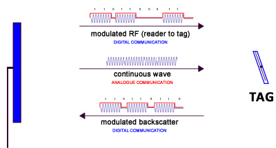
RFID systems operate according to one of two basic procedures:
full-duplex (FDX)/half-duplex (HDX) systems, and sequential systems (SEQ).
In full-duplex and half-duplex systems the transponder’s response is broadcast when the reader’s RF field is switched on.
Because the transponder’s signal to the receiver antenna can be extremely weak in comparison with the signal from the reader itself,
appropriate transmission procedures must be employed to differentiate the transponder’s signal from that of the reader.
In practice, data transfer from transponder to reader takes place using load modulation, load modulation using a subcarrier,
and also (sub)harmonics of the reader’s transmission frequency.
In contrast, sequential procedures employ a system whereby the field from the reader is switched off briefly at regular intervals.
These gaps are recognised by the transponder and used for sending data from the transponder to the reader.
The disadvantage of the sequential procedure is the loss of power to the transponder during the break in transmission,
which must be smoothed out by the provision of sufficient auxiliary capacitors or batteries.
This kind of sequential communications protocol contrasts with full-duplex and half-duplex communications,
which transmit the energy-providing carrier continuously while exchanging information simultaneously (full-duplex)
or in alternating periods (half-duplex) (see Fig. 4).
Representation of full duplex, half duplex and sequential systems over time.
Data transfer from the reader to the transponder is termed downlink,
while data transfer from the transponder to the reader is termed uplink
Fig. 4: Energy transfer through RF signal transmission occurs continuously in full-duplex (FDX) and half-duplex (HDX) communications,
but bursts in sequential (SEQ) systems such as RFID tags that use such power cycles to charge a capacitor for peak power demand.
Data transfer from the reader (down link) or from the tag (up link) occurs simultaneously
with FDX or in alternating periods with HDX and SEQ methods. (Source: Tektronix.)

HDX and FDX
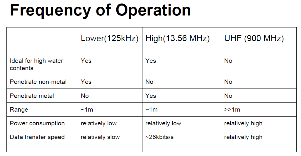
Low Frequency RFID uses magnetic fields to wirelessly power a passive tag so it can transmit an identification number. Magnetic signals can travel through most non-metallic materials, including water, wood, plastic, glass, concrete, and dirt. HF and UHF radio signals do not conduct well through water so LF RFID is the ideal choice for fish and wildlife tracking.
The ISO 11784/11785 standard specifies protocols so that tags and readers from different manufacturers will work together. FDX and HDX are interoperable but not compatible. Like AM and FM radios, there are PIT tag readers that detect FDX only, HDX only or both.
The two technologies have different strengths and capabilities so the choice depends on the how it will be used.
Half Duplex (HDX)
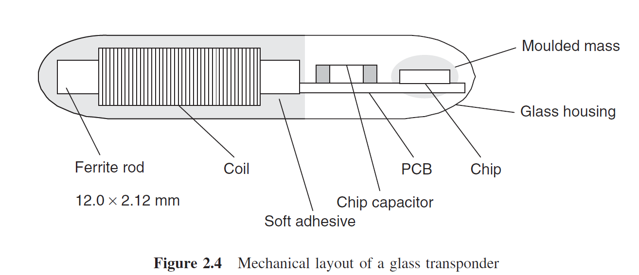
A half duplex RFID reader generates short magnetic pulses that wirelessly charge a capacitor inside an HDX tag. When the charge field turns off, the tag uses the stored power to send the tag number back to the reader without interference from the reader.
The capacitor in an HDX tag limits how small one can be made. Currently the smallest HDX tag is 12.0 mm x 2.15 mm.
HDX uses Frequency Shift Keying (FM) which has better noise immunity and allows larger, simpler antennas.
Antennas for HDX readers are very simple loops of insulated wire that can be placed directly in the water without an air gap or frame. Antennas for HDX can be 10 times larger than FDX ones. The largest known HDX antenna crosses a 190'/60 meter stream.
Since the charge field is pulsed, HDX readers require less power. The 50 ms/20 ms charge/listen cycle allows the scan rate of 14 per second. It is possible to shorten the charge pulse time to increase the speed up to 28 scans per second but the tag may not get fully charged.
Full duplex RFID generates a continuous magnetic field which powers the tag to respond immediately. Tags repeat their message while powered by the field, up to 30 times per second.
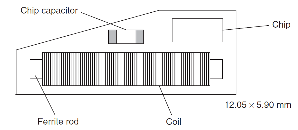
FDX tags can be made very small and thin due to their simple construction of a coil, ferrite rod and a chip. Very small tags have short a read range and so are primarily used for proximity or hand scanning.
FDX uses Amplitude Shift Keying (AM) and is susceptible to atmospheric noise which limits antenna sizes. FDX antennas in water must have an air gap around the wire that is held rigid to prevent movement due to vibration. Antennas are installed in large diameter plastic pipe or tubing for this purpose.
Dual mode readers can detect both kinds of tags by listening for FDX when the charge field is on and turning off every 50 ms to listen for an HDX tag. These readers must fit the requirements of both technologies so the antenna needs an air gap when placed in water and will be limited to FDX sizes.
Another possibility is to use separate FDX and HDX readers and antennas which can coexist with proper synchronization. This is more effort and cost but uses the advantages of the each technology.
Tag to Reader communication
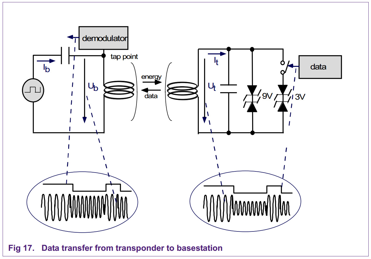
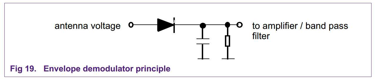
This amplitude modulation can be detected by a very basic and simple kind of demodulator, the so called envelope demodulator:
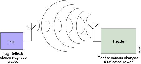
A backscatter tag communicates by modulating the scattered electromagnetic wave incident from the reader.
The scattered wave is modulated by changing the electrical impedance presented to the tag antenna.
A passive backscatter tag receives the power needed to operate from the wave incident from the reader.
Generation of load modulation in the transponder by switching the drain-source resistance of an FET on the chip.
The reader illustrated is designed for the detection of a subcarrier.
Shown is a RFID transceiver that communicates with a passive Tag.
Passive tags have no power source of their own and instead derive power from the incident electromagnetic field.
Commonly the heart of each tag is a microchip.
When the Tag enters the generated RF field it is able to draw enough power from the field
to access its internal memory and transmit its stored information.
When the transponder Tag draws power in this way the resultant interaction of the RF fields
causes the voltage at the transceiver antenna to drop in value.
This effect is utilized by the Tag to communicate its information to the reader.
The Tag is able to control the amount of power drawn from the field and by doing
so it can modulate the voltage sensed at the Transceiver according to the bit pattern it wishes to transmit.
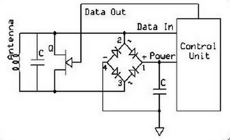

Sample circuit of the power supply and load modulator in a transponder
The voltage induced at the antenna coil L1 by the magnetic alternating field of the reader
is rectified using the bridge rectifier (D1–D4) and after additional smoothing (C1)
is available to the circuit as supply voltage. The parallel regulator (ZD 5V6) prevents
the supply voltage from being subject to an uncontrolled increase when the transponder approaches the reader antenna.
If the additional load resistor in the transponder is switched on and off at a very high elementary frequency fH,
then two spectral lines are created at a distance of ±fH around the transmission frequency of the reader,
and these can be easily detected (however fH must be less than fREADER).
In the terminology of radio technology the new elementary frequency is called a subcarrier.
Data transfer is by the ASK, FSK or PSK modulation of the subcarrier in time with the data flow.
This represents an amplitude modulation of the subcarrier.

Backscatter Coupling
We know from the field of RADAR technology that electromagnetic waves
are reflected by objects with dimensions greater than around half the wave length of the wave.
The efficiency with which an object reflects electromagnetic waves is described by its reflection cross-section.
Objects that are in resonance with the wave front that hits them,
as is the case for antenna at the appropriate frequency for example, have a particularly large reflection cross-section.
Backscatter Modulation:
Operating principle of a backscatter transponder.
The impedance of the chip is ‘modulated’ by switching the chip’s FET (Integrated Silicon Design, 1996)
BACKSCATTER MODULATION
This terminology refers to the communication method used by a passive RFID tag to send data to the reader using the same reader’s carrier signal.
The incoming RF carrier signal to the tag is transmitted back to the reader with tag’s data.
The RF voltage induced in the tag’s antenna is amplitude-modulated by the modulation signal (data) of tag device.
This amplitude-modulation can be achieved by using a modulation transistor across the LC resonant circuit or partially across the resonant circuit.
The changes in the voltage amplitude of tag’s antenna can affect on the voltage of the reader antenna.
By monitoring the changes in the reader antenna voltage (due to the tag’s modulation data), the data in the tag can be reconstructed.
The RF voltage link between reader and tag antennas are often compared to a weakly coupled transformer coils;
as the secondary winding (tag coil) is momentarily shunted, the primary winding (reader coil) experiences a momentary voltage drop.
Backscatter is one of the most widely used modulation schemes for modulating data on to rf carrier.
In this method of modulation, the tag coil (load) is shunted depending on the bit sequence received.
This in turn modulates the rf carrier amplitude as shown in the diagram below.
The reader detects the changes in the modulated carrier and recovers the data.
The above diagram provides a simplified modulated carrier signals from the RFID tag.
As seen in the diagram, the encoded binary digits modulate rf carrier.
A 1 is represented with high carrier level, and a 0 is represented by a low carrier level (tag coil shunted).
The reader demodulates the signals to recover the data, and note that this data is still encoded.
The reader decodes the data using suitable decoder,
and forwards it for further processing to a computer (or any backend server).

Operation principle of a backscatter transponder
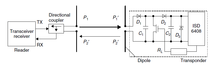
Power P1 is emitted from the reader‘s antenna, a small proportion of which (free space attenuation) reaches the transponder‘s antenna.
The power P1‘ is supplied to the antenna connections as HF voltage and after rectification by the diodes D1 and D2
this can be used as turn on voltage for the deactivation or activation of the power saving "power-down" mode.
The diodes used here are low barrier Schottky diodes, which have a particularly low threshold voltage.
The voltage obtained may also be sufficient to serve as a power supply for short ranges.
A proportion of the incoming power P1‘ is reflected by the antenna and returned as power P2.
The reflection characteristics (= reflection cross-section) of the antenna can be influenced by altering the load connected to the antenna.
In order to transmit data from the transponder to the reader,
a load resistor RL connected in parallel with the antenna is switched on and off in time with the data stream to be transmitted.
The amplitude of the power P2 reflected from the transponder can thus be modulated (modulated backscatter).
The power P2 reflected from the transponder is radiated into free space.
A small proportion of this (free space attenuation) is picked up by the reader‘s antenna.
The reflected signal therefore travels into the antenna connection of the reader in the "backwards direction"
and can be decoupled using a directional coupler and transferred to the receiver input of a reader.
The "forward" signal of the transmitter, which is stronger by powers of ten, is to a large degree suppressed by the directional coupler.
The ratio of power transmitted by the reader and power returning from the transponder (P1 / P2) can be estimated using the radar equation

Lets take an example of passive transponder data transmission which sends out data at frequency of 134.2kHz.
Reader or so called interrogator sends out 134.2kHz pulse which lasts for 50ms which is used
to power passive tag and start up the transponder controller.
Received energy is stored in cap pacitor inside transponder.
After this 50ms pulse ends, transponder transmits data back over period 20ms.
After tag transmitting is over, capacitor discharges and resets for next readings.
Passive Tag transmission is usually performed by switching low resistance across the antenna coil.
The change of voltage across antenna generates radio frequency which is referred as backscattering.
Data is read from tags ROM memory and transmitted serially by switching coil load switch.
Coil switch is driven by carrier clock source which is modulated with data from serial ROM memory data.
In other end the reader removes(demodulates) the carrier signal, filters and cleans up the signal with Schmitt trigger.
Then signal enters digital section, where CRC code is checked and decoded.
Passive RFID tags vary in how they communicate data to RFID readers and
how they receive power from the RFID reader's inductive or electromagnetic field.
This is commonly performed via two basic methods:

Passive Tag Load Modulation
Load modulation and inductive coupling in the near field—In this approach,
the RFID reader provides a short-range alternating current magnetic field
that the passive RFID tag uses for both power and as a communication medium.
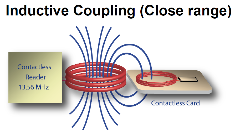
Via a technique known as inductive (or near-field) coupling ,
this magnetic field induces a voltage in the antenna coil of the RFID tag,
which in turn powers the tag.
The tag transmits its information to the RFID reader by taking advantage of the fact
that each time the tag draws energy from the RFID reader's magnetic field,
the RFID reader itself can detect a corresponding voltage drop across its antenna leads.
Capitalizing on this phenomenon, the tag can communicate binary information to the reader
by switching ON and OFF a load resistor to perform load modulation.
When the tag performs load modulation, the RFID reader detects this action
as amplitude modulation of the signal voltage at the reader's antenna.
Load modulation and inductive coupling can be found among passive RFID tags
using frequencies from 125 to 135 kHz and 13.56 MHz.
Limitations that exist with regard to the use of such low frequencies include the necessity to use larger antennas,
low data rate and bandwidth and a rather dramatic decay in the strength of the electromagnetic field (1/r6),
where r represents the distance between a low frequency interrogator and a passive RFID tag.
Ohmic Load Modulation
Equivalent circuit diagram for a transponder with load modulator.
Switch S is closed in time with the data stream – or a modulated subcarrier signal – for the transmission of data
Capacitive Load Modulation
Equivalent circuit diagram for a transponder with capacitive load modulator.
To transmit data the switch S is closed in time with the data stream – or a modulated subcarrier signal
Passive Tag Backscatter Modulation
Backscatter modulation and electromagnetic coupling in the far field—In this approach),
the RFID reader provides a medium-range electromagnetic field that the passive RFID tag
uses for both power and a communication medium.
Via a technique known as electromagnetic (or far-field) coupling,
the passive RFID tag draws energy from the electromagnetic field of the RFID reader.
However, the energy contained in the incoming electromagnetic field
is partially reflected back to the RFID reader by the passive tag antenna.
The precise characteristics of this reflection depend on the load (resistance)connected to the antenna.
The tag varies the size of the load that is placed in parallel with the antenna
in order to apply amplitude modulation to the reflected electromagnetic waves,
thereby enabling it to communicate information payloads back to the RFID reader via backscatter modulation.
Tags using backscatter modulation and electromagnetic coupling typically
provide longer range than inductively coupled tags, and can be found most commonly among
passive RFID tags operating at 868 MHz and higher frequencies.
Far field coupled tags typically provide significantly longer range than inductively coupled tags,
principally due to the much slower rate of attenuation (1/r2) associated with the electromagnetic far-field.
Antennas used for tag employing far field coupling are typically smaller than their inductively coupled counterparts.

Backscatter Modulation in Semi-Passive RFID Tags
Semi-passive RFID tags overcome two key disadvantages of pure passive RFID tag designs:
•![]() The lack of a continuous source of power for onboard telemetry and sensor asset monitoring circuits.
The lack of a continuous source of power for onboard telemetry and sensor asset monitoring circuits.
•![]() Short range.
Short range.
Semi-passive tags differ from passive tags in that they use an onboard battery
to provide power to communication and ancillary support circuits,
such as temperature and shock monitoring.
It is interesting to note that although they employ an onboard power source,
semi-passive RFID tags do not use it to directly generate RF electromagnetic energy.
Rather, these tags typically make use of backscatter modulation and
reflect electromagnetic energy from the RFID reader to generate a tag response
similar to that of standard passive tags.
The onboard battery is used only to provide power for telemetry
and backscatter enabling circuits on the tag, not to generate RF energy directly.

Reader to tag communication
A digitally modulated signal is a stream of distinct symbols.
A simple example with substantial relevance for RFID is on/off keying (OOK).
On-Off Keying (OOK)
Most current optical transmission systems encode the signal as a sequence of light pulses in a binary form.
This is called “on-off keying” (OOK).
Sometimes this is described as amplitude modulation, comparing it to AM radio.
In fact, the technique is nothing like AM radio.
An AM radio carries an analogue signal.
The amplitude of the carrier is continuously varied (modulated) in accordance with variations in the signal.
The receiver recovers the signal from the variations of the carrier.
But in an optical system, it is much more like a very simple form of digital baseband transmission in the electronic world.
The signal is there or it isn’t; beyond this the amplitude of the signal doesn’t matter.
In fairness, you can call OOK a special case of amplitude shift keying (ASK)
in which a number of discrete signal amplitude levels are used to carry a digital signal.
The signal power is kept large (m = 1) to indicate a binary '1'
and small or zero (m = 0) to represent a binary '0'.
An example is shown in Figure 3.6. In OOK, each symbol is a period of fixed duration
in which the signal power is either high or low.
Each OOK symbol represents one binary bit, though other types of symbols can convey more than one bit each.
Any circuit that can change the output power, such as a simple switch,can be used to create an OOK signal,
and any circuit that can detect power levels can demodulate (extract the data from) the signal.
For example, a diode (an electrical component that passes electrical current only in one direction
and blocks current flow in the opposite direction) can rectify a high-frequency signal, turning it into pulses of DC.
These pulses can be smoothed with a storage capacitor to produce an output signal that looks very much like the baseband signal m(t).
If the diode responds rapidly, it can be used at very high frequencies.
Modern diodes can operate up to over 1 GHz, allowing passive RFID tags to demodulate a reader signal using only a diode and capacitor.
Unmodified OOK is admirably simple and seems promising as a method of modulating a reader signal.
However, there is a problem with OOK for passive RFID.
A passive RFID tag depends on power obtained from the reader to run its circuitry.
If that power is interrupted, the tag cannot operate.
However, imagine the case of an OOK signal containing a long string of binary 0s:
in this case, m = 0 for as long as the data remains 0.
The tag will receive no power during this time.
If the data remains '0' for too long, the tag will power off and need to be restarted,
a situation not likely to be conducive to reliable operation.
Even when some binary 1s are present, the power level delivered to the tag is strongly data dependent, an undesirable trait.
(Figure 3.7) Pulse-interval Coding Baseband Symbols (the function m(t))
A common solution to the power problem is to code the binary data prior to modulation.
One RFID coding approach is known as pulse-interval encoding (PIE).
A binary '1' is coded as a short power-off pulse following a long full-power interval,
and a binary '0' is coded as a shorter full-power interval with the same power-off pulse (Figure 3.7).
The resulting coded baseband signal m(t) is then used to modulate the carrier (Figure 3.8).
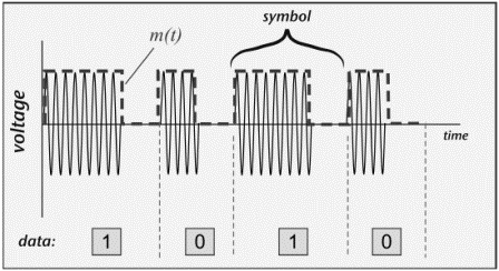
Figure 3.8 Pulse-interval Coding with OOK Modulation of a Carrier Wave

PIE using equal low and high pulses for a '0' ensures that at least 50% of the maximum power
is delivered to the tag even when the data being transmitted contains long strings of zeros,
and if the high is three times as long for a '1', a random stream of equally mixed binary data
will provide about 63% of peak power. Note that in this case, the data rate becomes dependent on the data:
a stream of binary 0s will be transmitted more rapidly than a stream of binary 1s.
A single symbol has two features—the off-time and on-time—but still conveys only one binary bit.
(This scheme is used in EPCglobal Class 1 Generation 2 readers.
Other passive RFID standards use slightly different coding schemes,
all generally characterized by the desire to have the reader power on as much as possible to power the tag.)
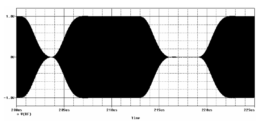
Reader RF signal, 100% modulation

Reader RF signal, 20% modulation
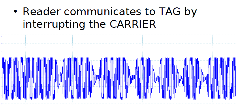
Data transfer reader → transponder
Data is sent in driection from basestation to transponder by modulatating the magnetic field ("On/Off Keying, 100% modulation)
respectively switching off the field for short periods of time.
During that time, the transponder energy and clock supply is provided by transponder resonant circuitry.
The data is coded into the postion and/or distance of these field gaps.
A field gap is started by switching off the antenna drivers.
After this, the energy stored in the basestation antenna resonant circuitry is cut down by clipping diodes in driver stages.
Therefore the field strength decays rapidly to zero.
After switching the drivers on again, the resonance circuitry energy has to be build up again.
The time needed for that depends on the quality factor of the antenna.

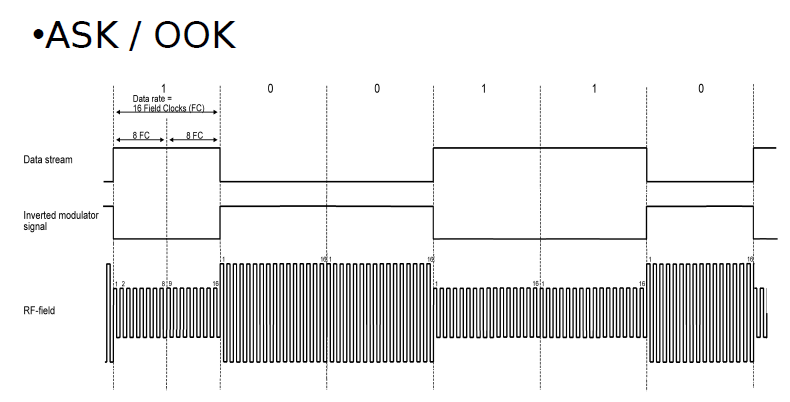
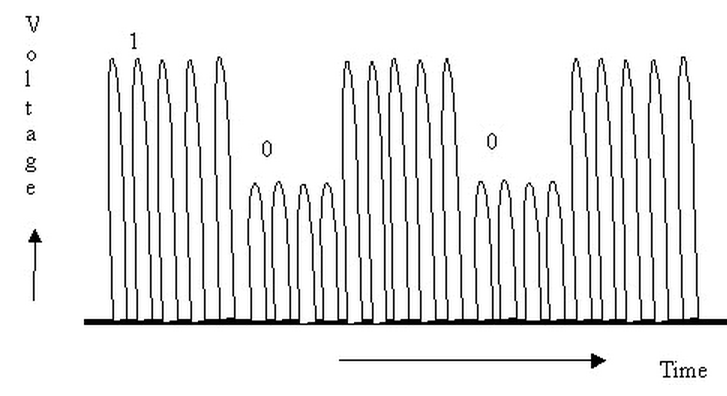
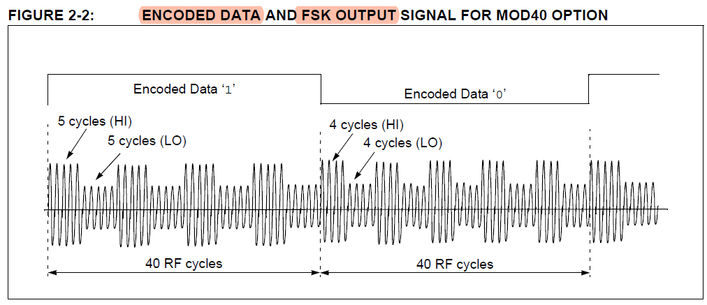
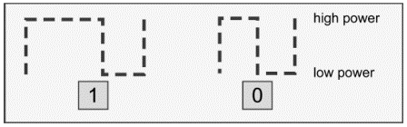
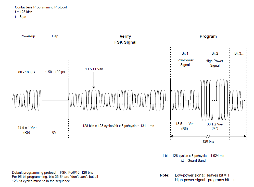
DATA MODULATION FOR 125 kHz DEVICES
Although all the data is transferred to the host by amplitude-modulating the carrier (backscatter modulation),
the actual modulation of 1’s and 0’s is accomplished with three additional modulation methods:
1. Direct.
In direct modulation, the Amplitude Modulation of the backscatter approach is the only modulation used.
A high in the envelope is a ‘1’ and a low is a ‘0’. Direct modulation can provide a high data rate but low noise immunity.
2. FSK (Frequency Shift Keying).
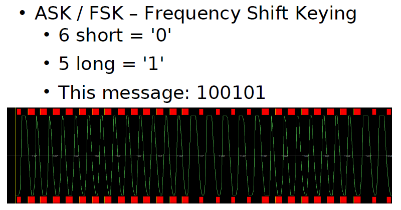
This form of modulation uses two different frequencies for data transfer; the most common FSK mode is FC/8/10.
In other words, a ‘0’ is transmitted as an amplitude-modulated clock cycle with period corresponding to the carrier frequency divided by 8,
and a ‘1’ is transmitted as an amplitude-modulated clock cycle period corresponding to the carrier frequency divided by 10.
The amplitude modulation of the carrier thus switches from FC/8 to FC/10 corresponding to 0’s and 1’s in the bitstream,
and the reader has only to count cycles between the peak-detected clock edges to decode the data.
FSK allows for a simple reader design, provides very strong noise immunity,
but suffers from a lower data rate than some other forms of data modulation.
In Figure 3, FSK data modulation is used with NRZ encoding.
3. PSK (Phase Shift Keying).
This method of data modulation is similar to FSK, except only one frequency is used,
and the shift between 1’s and 0’s is accomplished by shifting the phase of the backscatter clock by 180 degrees.
Two common types of PSK are:
• Change phase at any ‘0’, or
• Change phase at any data change (0 to 1 or 1 to 0).
PSK provides fairly good noise immunity, a moderately simple reader design, and a faster data rate than FSK.
Typical applications utilize a backscatter clock of FC/2, as shown in Figure 4.
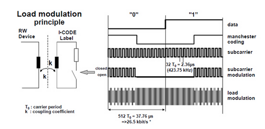
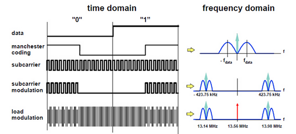
這個例項是ISO/IEC 15693-2中的內容是關於標籤向reader的通訊的調製過程。
如圖所示,標籤需要傳送的訊號為“0”和“1”,其數字波形如圖上的data;
通過曼徹斯特編碼後為圖上所示的manchester coding的數字波形;
subcarrier為副載波,其目的也是以提高資訊傳輸的可靠性;
最終要發出去的數字訊號就變成了subcarrier modulation的數字波形;
而最終發給Reader端的資料是一個射頻訊號,標籤通過負載調製發射出的最終訊號為13.56MHz載波的訊號load modulation的訊號。
Coding in the Baseband
Non-return to Zero Modulation (NRZ)
Low level = 0V
High level = +V
For each bit, there are n clocks (data rate).
Requires time co-ordination:
Longs strings of ‘0’ and ‘1’ do not produce any transitions which may create problems in error detection and recovery.
High DC level ( average of ½ Volts ).
Return to Zero Modulation (RZ)
Low level = 0V
High level = +V during the first half of the bit and 0 during the second half.
DC average is only ¼ Volts.
Requires time co-ordination
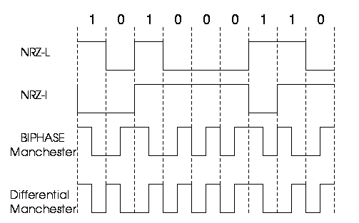
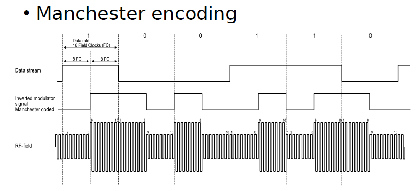
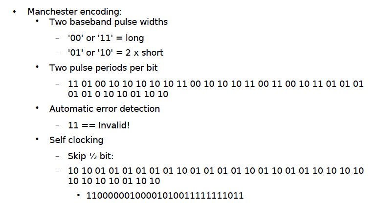
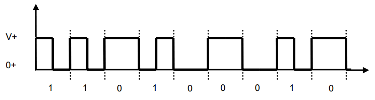
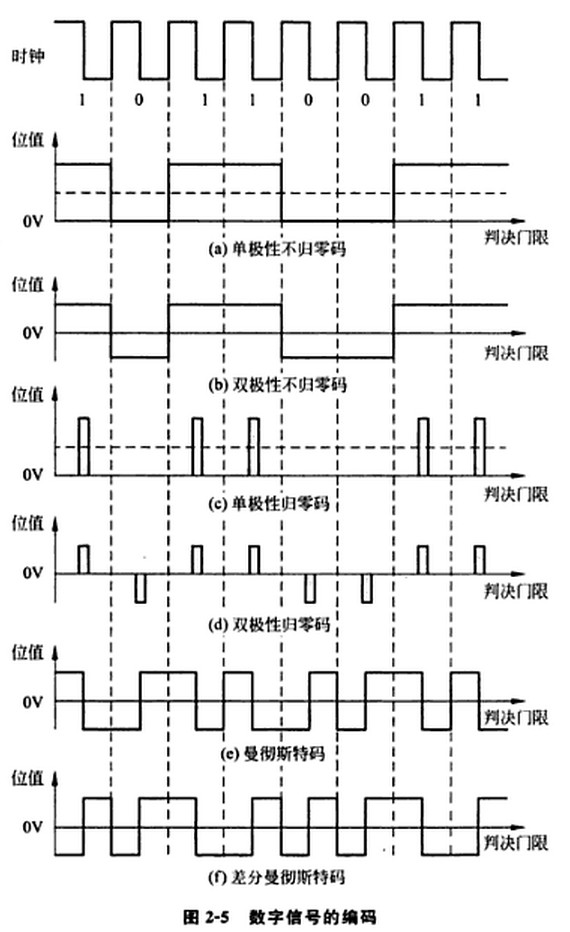
Manchester Coding
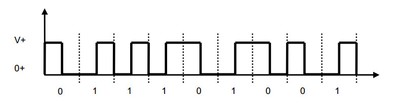
This code is self-clocking
There is a transition at the start of the bit period, if the bit '0' is followed by a '0' bit or the bit '1' is followed by a '1' bit
There is no transition at the start of the bit period, if the bit is '0', followed by a '1' bit or the bit '1' is followed by a '0' bit
There is a transition in the middle of each bit period
A 1 to 0 transition represents a '0' bit
A 0 to 1 transition represents a '1' bit
The mid-bit transition is used as clock as well as data.
The residual DC value is eliminated by having both polarities for every bit
The bandwidth required could be twice the bit rate (Efficiency of this code can be as low as 50%)
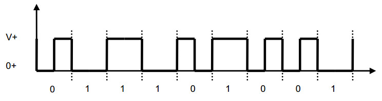
Differential Manchester Coding <HITAG : MANCHESTER>
This code is self-clocking
A transition at the start of the bit period represents a '0' bit
No transition at the start of the bit period represents a '1' bit
There is a transition in the middle of each bit period
The mid-bit transition is used only to provide clocking.
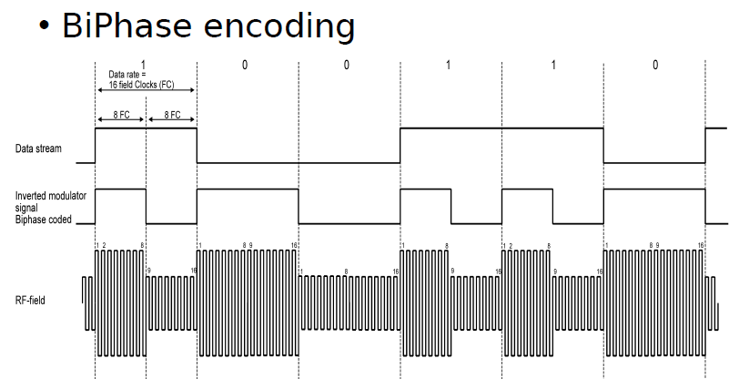
Biphase Coding <Biphase Mark Coding : BMC >
Biphased data streams have generally a signal change in the middle of each bit, independent of the value.
Therefore the signal does not necessarily return to zero.
The advantages of the biphase method are:
Synchronisation : Since there is a predictable transition for each bit, the beceiver can synchronise on this edge.
These codes are also known as self-clocking
Error immunity : To cause an error, the noise must invert both, the signal before and after the transition
There is a transition at the start of each bit period
A '0' has no transition in the middle of the bit period
A '1' bit has generally a transition in the middle of the bit period (pos. or neg.)
Differential Biphase Coding < HITAG : BIPHASE >
There is a transition at the start of each bit period
A '0' bit has generally a transition in the middle of the bit period (pos. or neg.)
A '1' has no transition in the middle of the bit period
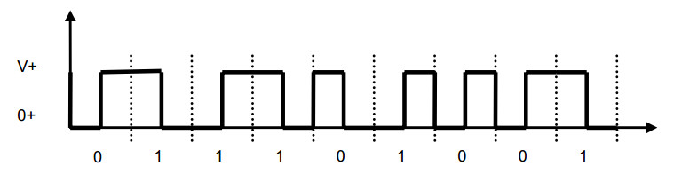
Miller Coding
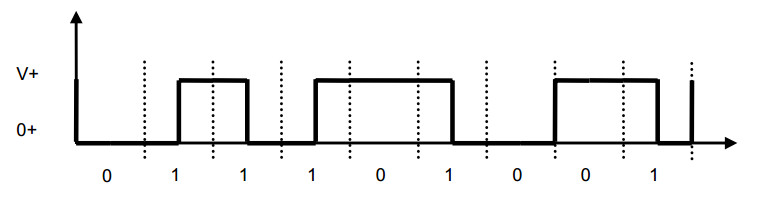
There is a transition at the start of the bit period, if the bit '0' is followed by a '0' bit
There is no transition at the start of the bit period, if the bit is '0', followed by a '1' bit
There is a transition in the middle of a bit period, if it is a bit '1'
This code is very efficient, regarding the desired bandwidth (half of the desired bandwidth of Manchester Coding).
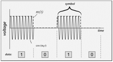
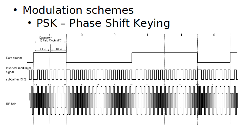
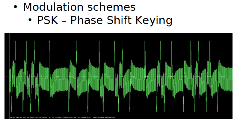
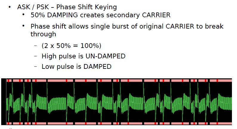
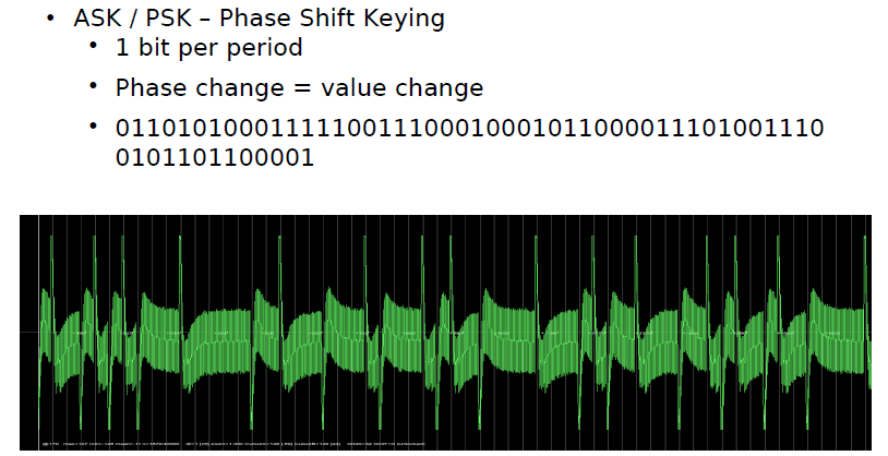
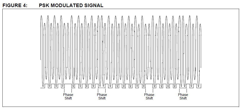
Phase Shift Keying
Phaseshift keyed data is only decodable with angle sensitive demodulators. The data information can be found in the phase of the signal.
AM demodulators will show no results.
A bit '1' has a signal phase of π or 180°
A bit '0' has a signal phase of 0°
The interpretation of the digital value can as well be interpreted inverse ('1' → π, '0' → 180°).
The conventional understanding of PSK is shown in the following figure, where the carrier is modulated by the transmitter (reader).
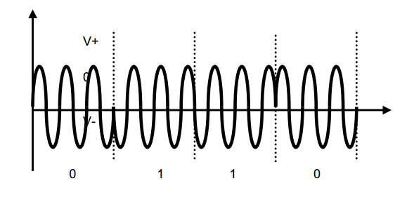
PSK modulation is also possible if the carrier is quasi-amplitude-modulated by the transponder as principally shouwn in the following figure.
The above example shows a PSK modulation with two periods per bit of data information.
The upper trace is the control of the transponder modulator.

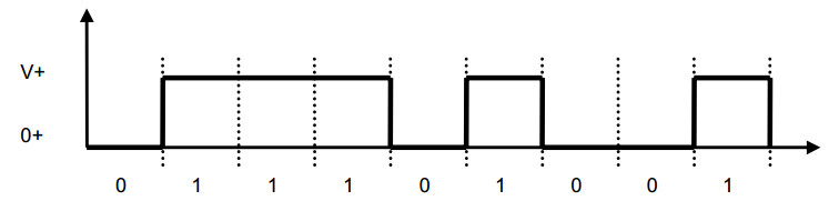
DATA ENCODING
Data encoding refers to processing or altering the data bitstream in-between the time it is retrieved
from the RFID chip’s data array and its transmission back to the reader.
The various encoding algorithms affect error recovery, cost of implementation, bandwidth,
synchronization capability and other aspects of the system design. Entire textbooks are written on the subject, but
there are several popular methods used in RFID tagging today:
1. NRZ (Non-Return to Zero) Direct.
In this method no data encoding is done at all; the 1’s and 0’s are clocked from the data array directly to the output transistor.
A low in the peak-detected modulation is a ‘0’ and a high is a ‘1’.
2. Differential Biphase.
Several different forms of differential biphase are used, but in general the bitstream being clocked out of the data array is modified
so that a transition always occurs on every clock edge, and 1’s and 0’s are distinguished by the transitions within the middle of the clock period.
This method is used to embed clocking information to help synchronize the reader to the bitstream.
Because it always has a transition at a clock edge, it inherently provides some error correction capability.
Any clock edge that does not contain a transition in the data stream is in error and can be used to reconstruct the data.
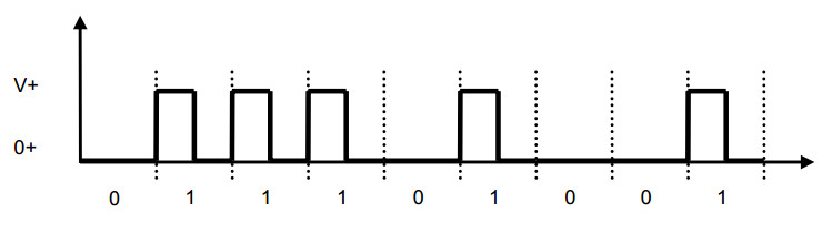
3. Biphase_L (Manchester).
This is a variation of biphase encoding in which there is not always a transition at the clock edge.
The MCRF355/360 and MCRF45X devices use this encoding method.
http://en.wikipedia.org/wiki/Return-to-zero
RZ 編碼(Return-to-zero Code),即歸零編碼。
在 RZ 編碼中,正電平代表邏輯 1,負電平代表邏輯 0,並且,每傳輸完一位資料,訊號返回到零電平,
也就是說,訊號線上會出現 3 種電平:正電平、負電平、零電平:

從圖上就可以看出來,因為每位傳輸之後都要歸零,所以接受者只要在訊號歸零後取樣即可,這樣就不在需要單獨的時鐘訊號。
實際上,RZ 編碼就是相當於把時鐘訊號用歸零編碼在了資料之內。這樣的訊號也叫做自同步(self-clocking)訊號。
這樣雖然省了時鐘資料線,但是還是有缺點的,因為在 RZ 編碼中,大部分的資料頻寬,都用來傳輸“歸零”而浪費掉了。
Return-to-zero
Return-to-zero (RZ) describes a line code used in telecommunications signals in which the signal drops (returns) to zero between each pulse.
This takes place even if a number of consecutive 0s or 1s occur in the signal.
The signal is self-clocking. This means that a separate clock does not need to be sent alongside the signal,
but suffers from using twice the bandwidth to achieve the same data-rate as compared to non-return-to-zero format.
The "zero" between each bit is a neutral or rest condition, such as
a zero amplitude in pulse amplitude modulation (PAM),
zero phase shift in phase-shift keying (PSK), or
mid-frequency in frequency-shift keying(FSK).
That "zero" condition is typically halfway between the significant condition representing a 1 bit and the other significant condition representing a 0 bit.
Although return-to-zero (RZ) contains a provision for synchronization, it still has a DC component resulting in “baseline wander”
during long strings of 0 or 1 bits, just like the line code non-return-to-zero.
Return to zero, inverted
Return-to-zero, inverted (RZI) is a method of mapping for transmission.
The two-level RZI signal has a pulse (shorter than a clock cycle) if the binary signal is 0, and no pulse if the binary signal is 1.
It is used (with a pulse 3/16 of a bit long) by the IrDA serial infrared (SIR) physical layer specification.
Required bandwidth for this kind of modulation is: BW = R(data rate)
http://en.wikipedia.org/wiki/Non-return-to-zero
http://zh.wikipedia.org/wiki/%E4%B8%8D%E6%AD%B8%E9%9B%B6
NRZ 編碼(Non-return-to-zero Code),不歸零編碼。
我們去掉這個歸零步驟,NRZ 編碼(Non-return-to-zero Code)就出現了,和 RZ 的區別就是 NRZ 是不需要歸零的:
http://baike.baidu.com/view/491480.htm
歸零碼

單極性歸零碼
雙極性歸零碼
Non-return-to-zero
NRZ指的是在一個位元位的傳送時間內,電壓是保持不變的(比如說,不回到零點)。
In telecommunication, a non-return-to-zero (NRZ) line code is a binary code in which
1s are represented by one significant condition (usually a positive voltage) and
0s are represented by some other significant condition (usually a negative voltage), with no other neutral or rest condition.
The pulses have more energy than a return-to-zero (RZ) code.
Unlike RZ, NRZ does not have a rest state.
NRZ is not inherently a self-clocking signal, thus some additional synchronization technique
(for example a run length limited constraint, or a parallel synchronization signal) must be used for avoiding bit slip.
For a given data signaling rate, i.e., bit rate, the NRZ code requires only half the baseband bandwidth required
by the Manchester code (the passband bandwidth is the same).
When used to represent data in an asynchronous communication scheme,
the absence of a neutral state requires other mechanisms for bit synchronization
when a separate clock signal is not available.
NRZ-Level itself is not a synchronous system but rather an encoding that can be used
in either a synchronous or asynchronous transmission environment,
that is, with or without an explicit clock signal involved.
Because of this, it is not strictly necessary to discuss how the NRZ-Level encoding acts "on a clock edge" or "during a clock cycle"
since all transitions happen in the given amount of time representing the actual or implied integral clock cycle.
The real question is that of sampling—the high or low state will be received correctly provided the transmission line has stabilized for that bit
when the physical line level is sampled at the receiving end.
However, it is helpful to see NRZ transitions as happening on the trailing (falling) clock edge in order to compare NRZ-Level to other encoding methods,
such as the mentioned Manchester code, which requires clock edge information (is the XOR of the clock and NRZ, actually)
see the difference between NRZ-Mark and NRZ-Inverted.
在電信學中,不歸零編碼 (non-return-to-zero line code, NRZ) 指的是一種二進位制的訊號程式碼,
在這種傳輸方式中,1 和 0 都個別由不同的電子顯著狀態來表現,除此之外,沒有中性狀態、亦沒有其他種狀態。
這種脈衝的能量比歸零程式碼要來得密集,但它傳輸時是不停歇的,這代表同步訊號必須在此程式碼之外獨自傳輸。
在給定一個訊號頻率的情況下(比如說位元率),NRZ 程式碼只需要曼徹斯特程式碼 (Manchester code) 的一半頻寬。
當用於非同步傳輸時,由於缺少中性狀態,必須依靠其他種機制,來達成在同步傳輸中使用時鐘偵測錯誤的資料回覆工作。
NRZ-Level 本身並非一種同步系統,而更是一種編碼方式,因為它可用於同步環境、或非同步環境中,也就是不管有沒有明確的時鐘訊號,都可以運作。
所以,討論 NRZ-Level 編碼是否在時鐘“跳動 (clock-edge)”或“跳動之間 (between clock-edge)”並非必要的,
因為每一個訊號一定都是以給定的時脈來傳輸的,這就暗示了訊號內在的時脈。
真正的問題是,能否在接收端以當初取樣時的同樣頻率重繪該訊號。
然而,由於 NRZ 訊號的脈衝與時鐘是一致的,這就很容易看出 NRZ-Level 和其他編碼方式的不同,
例如前面提到的曼徹斯特程式碼,它需要明確的時脈資訊(即 NRZ 和時鐘的 XOR 值),
還能看出與 NRZ-Mark 和 NRZ-Inverted 等編碼的不同。
不歸零法編碼 不歸零法(Nonreturn to Zero, NRZ)可能是最簡單的一種編碼方案。
它傳送一個0時把電壓升高,而傳送一個1時則使用低電平。
這樣,通過在高低電平之間作相應的變換來傳送0和1的任何序列。
NRZ指的是在一個位元位的傳送時間內,電壓是保持不變的(比如說,不回到零點)。
下圖描述了二進位制串1 0 1 0 0 11 0的NRZ傳輸過程。
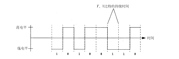
NRZ編碼雖然簡單,但卻存在一個問題。研究一下下圖中的傳輸。它正在傳送什麼呢?

你可以回答說是“一個0的序列”。是的,但到底有多少個0呢?
對於這個問題,你會回答說這取決於一個位元位的持續時間。
現在假設我們告訴你1毫米線段對應於一個週期。那麼你所要做的就是量出圖中線段的長度,並轉換為毫米。
這一計算將告訴你線段中有多少個1毫米的分段,也就是0的個數。理論上這個方法是行得通的,但實際上卻不然。
假設有個人用尺子畫出了一條包含1 0 0 0個1毫米分段的線段。那麼總共有多長呢?
答案是1米,但由於在測量和實際繪製時出現的誤差,線段可能只是接近而不是剛剛好一米長。
因此,當第二個人來測量這條線段時,他將得出一個比1 0 0 0個分段稍微多點或少點的答案。
即使第一個人很幸運,他的測量準確無誤,但第二個人度量時的不精確也將導致誤差。
這會給資料傳輸帶來什麼影響呢?
當一臺裝置傳送一個位元的數字訊號時,它將在一定的週期內,假定為T,產生一個持續的訊號。
一個內建的時鐘負責定時。接收裝置必須知道訊號的週期,這樣它才能在每個T時間單元內對訊號進行取樣。
它也有一個負責定時的內建時鐘。剩下的就是確保兩個時鐘使用同樣的T。
下一個問題是:所有的時鐘總是保持一致的嗎?任何物理裝置都存在著設計上的侷限性和缺陷。
幾乎可以肯定任何兩個時鐘都存在著微小的差別,這使得裝置無法對傳輸訊號作十分精確的取樣。
就好象我們在新年的第一天校正了兩個時鐘,但到了年底卻發現它們已經有了輕微的差別。
同樣地,管絃樂隊的音樂家們以同樣的速度同時開始演奏,但如果他們不看指揮,
也不注意聽別人的拍子的話,他們的節奏將開始混亂。
稍微的不和諧就將毀掉整個演奏,使它聽起來就象作者和他的同事們正在表演一樣。
就象指揮家確保演奏者的同步一樣,通訊裝置也需要某種機制以使它們的定時保持一致。
不變的訊號不具備同步機制。但如果訊號改變的話,這種改變就可以用來保持裝置的同步。
有些強制訊號改變的編碼方案就是基於這個原因。
Non return to zero(NRZ)
NRZ codes share the property that voltage level is constant during a bit interval.
High level voltage = bit 1 and Low level voltage = bit 0.
A problem arises when there is a long sequence of 0s or 1s and the volatage level
is maintained at the same value for a long time.
This creates a problem on the recieving end because now, the clock synchronization is lost due to lack of any transitions and hence,
it is difficult to determine the exact number of 0s or 1s in this sequence.
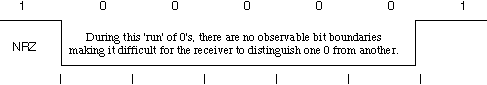
The two variations are as follows:
- NRZ-Level: In NRZ-L encoding, the polarity of the signal changes only when the incoming signal changes from a 1 to a 0 or from a 0 to a 1.
NRZ-L method looks just like the NRZ method, except for the first input one data bit.
This is because NRZ does not consider the first data bit to be a polarity change, where NRZ-L does. - NRZ-Inverted: Transition at the beginning of bit interval = bit 1 and No Transition at beginning of bit interval = bit 0 or vicecersa.
This technique is known as differential encoding.
NRZ-I has an advantage over NRZ-L.
Consider the situation when two data wires are wrongly connected in each other's place.
In NRZ-L all bit sequences will get reversed (B'coz voltage levels get swapped).
Whereas in NAZ-I since bits are recognized by transition the bits will be correctly interpreted.
A disadvantage in NRZ codes is that a string of 0's or 1's will prevent synchronization of transmitter clock
with receiver clock and a separate clock line need to be provided.
Unipolar non-return-to-zero level
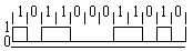
"One" is represented by one physical level (such as a DC bias on the transmission line).
"Zero" is represented by another level (usually a negative voltage).
"zero" transitions or remains low on the trailing clock edge of the previous bit, or just the opposite.
單極 NRZ-Level
1”由一種物理電平表現,例如傳輸線上的直流偏移 (DC bias)。
“0”由另一種電平表現(通常是負電壓)。
在時脈術語中,通常“1”沿著上一個位元的時脈邊緣,維持或改變到一個較低的位置;
而“0”則沿著上一個位元的時脈邊緣,維持或改變到一個較高的位置,或者兩者反過來。
這可能會造成一長串不改變的電平,讓同步工作變得困難。
一個解決辦法是隻傳送有著許多變化的訊號,見限制遊長 (Run Length Limited)。
圖表顯示最低一條線代表真正的零電平,而其上是代表“0”的邏輯電平,電壓代表“1”,這種配置較稀少。
Bipolar non-return-to-zero level
"One" is represented by one physical level (usually a positive voltage).
"Zero" is represented by another level (usually a negative voltage).
In clock language, in bipolar NRZ-Level the voltage
"swings" from positive to negative on the trailing edge of the previous bit clock cycle.
An example of this is RS-232, where "one" is −12 V to −5 V and "zero" is +5 V to +12 V.
兩極 NRZ-Level
1”由一物理電平表現(通常是正電壓)。負電壓 ?
“0”由另一電平表現(通常是負電壓)。正電壓 ?
在時脈術語中,兩極的 NRZ-Level 電壓沿著上一個位元的時脈邊緣,從正轉向負。
這種訊號的例子是 RS-232,它的“1”是 -5v 至 -12V 之間、“0”是 +5V 至 +12V 之間。
Non-return-to-zero Mark
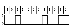
“1”由物理電平的改變來表示。
“0”由物理電平的沒有改變來表示。
在時脈術語中,沿著上一個位元的時脈邊緣作出改變的代表“1”,沒有改變的代表“0”。
觀看圖表來理解以改變為基礎的編碼時,必須理解到如果第一個位元之前的初始狀態被判斷為相反的,
則整個訊號會是反相的、或部份反相的。
在其他檔案中,這個編碼很常只用“NRZ”單名來稱呼[1];
FIPS 1037 也把“不歸零改變為一 (non-return-to-zero change-on-ones)
”和“不歸零一 (non-return-to-zero one)”定義為與此相同的東西。
Non-return-to-zero space
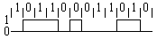
"One" is represented by no change in physical level.
"Zero" is represented by a change in physical level.
In clock language, the level transitions on the trailing clock edge of the previous bit to represent a "zero."
This "change-on-zero" is used by High-Level Data Link Control and USB.
They both avoid long periods of no transitions (even when the data contains long sequences of 1 bits) by using zero-bit insertion.
HDLC transmitters insert a 0 bit after five contiguous 1 bits (except when transmitting the frame delimiter '01111110').
USB transmitters insert a 0 bit after six consecutive 1 bits.
The receiver at the far end uses every transition —
both from 0 bits in the data and these extra non-data 0 bits — to maintain clock synchronization.
The receiver otherwise ignores these non-data 0 bits.
1”由物理電平的沒有改變來表現。
“0”由電平的改變來表現。
在時脈術語中,沿著前一個位元的時脈邊緣改變的電平代表的是“0”。
這個“改變為零”的應用例子是 High-Level Data Link Control 和 USB。
它們利用插入零位元來避免長串的未改變位元(即使資料中包含了大量的 1 位元序列)。
HDLC 傳輸器會在連續的五個 1 位元后面,自動插入一個 0 位元(一個例外是區塊定義符 "01111110")。
USB 傳輸器會在六個連續的 1 位元后,插入一個 0 位元。
接收端將使用每一個電平的轉換(不管是資料本身還是自動插入位元)來維持時脈的同步性,若不為同步,則這些插入 0 位元會被忽略。
Non-return-to-zero inverted (NRZI)
Non return to zero, inverted (NRZI) is a method of mapping a binary signal to a physical signal
for transmissionover some transmission media.
The two level NRZI signal has a transition at a clock boundary if the bit being transmitted is a logical 1,
and does not have a transition if the bit being transmitted is a logical 0.
"One" is represented by a transition of the physical level.
"Zero" has no transition.
Also, NRZI might take the opposite convention, as in Universal Serial Bus (USB) signalling,
when in Mode 1, in which a transition occurs when signaling zero, and a steady level when signaling a one.
The transition occurs on the leading edge of the clock for the given bit.
This distinguishes NRZI from NRZ-Mark.
However, even NRZI can have long series of zeros (or ones if transitioning on "zero"),
and thus clock recovery can be difficult unless some form of run length limited (RLL) coding is used in addition to NRZI.
Magnetic disk and tape storage devices generally use fixed-rate RLL codes,
while USB uses bit stuffing, which inserts an additional 0 bit after 6 consecutive 1 bits.
While bit stuffing is efficient, it results in a variable data rate
because it takes slightly longer to send a long string of 1 bits than it does to send a long string of 0 bits.
NRZ-Inverted (NRZI)
一改變:“1”為物理電平上的改變。“0”為沒有改變。
零改變:“0”為物理電平上的改變。“1”為沒有改變。
改變發生在當下位元的時鐘脈衝前緣。
但是,NRZI 會有長串的 0或1 位元出現,導致時脈回覆有困難,可以使用一些編碼技巧(例如遊長限制)來解決。
曼徹斯特程式碼永遠有時脈訊號,但傳輸效率比 NRZI 低。
NRZI 編碼被用於磁帶的錄音、CD的燒錄和標準 USB 的傳訊。
NRZI編碼方式。
訊號電平的一次反轉代表1,電平不變化表示0,並且在表示完一個碼元后,電壓不需回到0
不歸零制編碼是效率最高的編碼
缺點是存在傳送方和接收方的同步問題
單極性不歸零碼,無電壓(也就是元電流)用來表示"0",而恆定的正電壓用來表示"1"。
每一個碼元時間的中間點是取樣時間,判決門限為半幅度電平(即0.5)。
也就是說接收訊號的值在0.5與1.0之間,就判為"1"碼,如果在O與0.5之間就判為"0"碼。
每秒鐘傳送的二進位制碼元數稱為"碼速"。
雙極性不歸零碼,"1"碼和"0"碼都有電流,但是"1"碼是正電流,"0"碼是負電流,正和負的幅度相等,故稱為雙極性碼。
此時的判決門限為零電平,接收端使用零判決器或正負判決器,接收訊號的值若在零電平以上為正,判為"1"碼;若在零電平以下為負,判為"0"碼。
以上兩種編碼,都是在一個碼元的全部時間內發出或不發出電流(單極性),以及發出正電流或負電流(雙極性)。
每一位編碼佔用了全部碼元的寬度,故這兩種編碼都屬於全寬碼,也稱作不歸零碼NRZ (Non Return Zero)。
如果重複傳送"1"碼,勢必要連續傳送正電流;如果重複傳送"0"碼,勢必要連續不送電流或連續傳送負電流,
這樣使某一位碼元與其下一位碼元之間沒有間隙,不易區分識別。歸零碼可以改善這種狀況。
NRZI 編碼(Non-Return-to-Zero Inverted Code)和 NRZ 的區別就是
NRZI 用訊號的翻轉代表一個邏輯,訊號保持不變代表另外一個邏輯。
USB 傳輸的編碼就是 NRZI 格式,在 USB 中,電平翻轉代表邏輯 0,電平不變代表邏輯1(NRZI 遇 0 翻轉,遇 1 不變):
翻轉的訊號本身可以作為一種通知機制,而且可以看到,即使把 NRZI 的波形完全翻轉,
所代表的資料序列還是一樣的,對於像 USB 這種通過差分線來傳輸的訊號尤其方便.
現在再回到那個同步問題:的確,NRZ 和 NRZI 都沒有自同步特性,但是可以用一些特殊的技巧解決。
比如,先傳送一個同步頭,內容是 0101010 的方波,讓接受者通過這個同步頭計算出傳送者的頻率,
然後再用這個頻率來取樣之後的資料訊號,就可以了。
在 USB 中,每個 USB 資料包,最開始都有個同步域(SYNC),這個域固定為 0000 0001,
這個域通過 NRZI 編碼之後,就是一串方波(複習下前面:NRZI 遇 0 翻轉遇 1 不變),
接受者可以用這個 SYNC 域來同步之後的資料訊號。
此外,因為在 USB 的 NRZI 編碼下,邏輯 0 會造成電平翻轉,所以接受者在接受資料的同時,
根據接收到的翻轉訊號不斷調整同步頻率,保證資料傳輸正確.
但是,這樣還是會有一個問題,就是雖然接受者可以主動和傳送者的頻率匹配,但是兩者之間總會有誤差。
假如資料訊號是 1000 個邏輯1,經過 USB 的 NRZI 編碼之後,就是很長一段沒有變化的電平,
在這種情況下,即使接受者的頻率和傳送者相差千分之一,就會造成把資料取樣成 1001 個或者 999 個 1了。
USB 對這個問題的解決辦法,就是強制插 0,也就是傳說中的 bit-stuffing,
如果要傳輸的資料中有 7 個連續的 1,傳送前就會在第 6 個 1 後面強制插入一個 0,
讓傳送的訊號強制出現翻轉,從而強制接受者進行頻率調整。
接受者只要刪除 6 個連續 1 之後的 0,就可以恢復原始的資料了。
曼徹斯特編碼
曼徹斯特編碼(Manchester Code)用訊號的變化來保持傳送裝置和接收裝置之間的同步。
也有人稱之為自同步碼( Self-Synchronizing Code)。
為了避免上面 不變的訊號不具備同步機制 情況,它用電壓的變化來分辨0和1。
它明確規定,從高電平到低電平的跳變代表0,而從低電平到高電平的跳變代表1。
下圖給出了位元串0 1 0 11 0 0 1的曼徹斯特編碼。如圖所示,訊號的保持不會超過一個位元位的時間間隔。
即使是0或1的序列,訊號也將在每個時間間隔的中間發生跳變。
這種跳變將允許接收裝置的時鐘與傳送裝置的時鐘保持一致。
曼徹斯特編碼的一個缺點是需要雙倍的頻寬。也就是說,訊號跳變的頻率是NRZ編碼的兩倍。
曼徹斯特編碼(Manchester Encoding),也叫做相位編碼( Phase Encode,簡寫PE),
是一個同步時鐘編碼技術,被物理層使用來編碼一個同步位流的時鐘和資料。
它在乙太網媒介系統中的應用屬於資料通訊中的兩種位同步方法[1]裡的自同步法(另一種是外同步法),
即接收方利用包含有同步訊號的特殊編碼從訊號自身提取同步訊號來鎖定自己的時鐘脈衝頻率,達到同步目的。
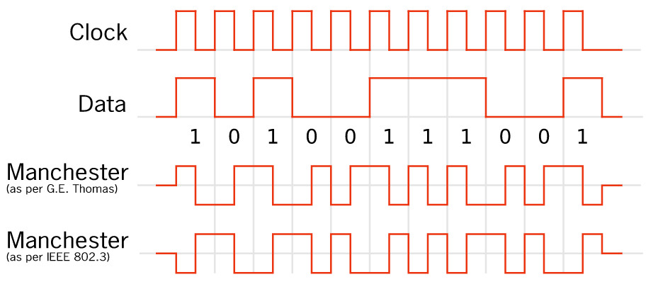
差分曼徹斯特編碼
和曼徹斯特編碼一樣,在每個位元時間間隔的中間,訊號都會發生跳變。
區別在於每個時間間隔的開始處。
0將使訊號在時間間隔的開始處發生跳變。而1將使訊號保持它在前一個時間間隔尾部的取值。( 不變 )
因此,根據訊號初始值的不同, 0將使訊號從高電平跳到低電平,或從低電平跳到高電平。
下圖給出了位元串1 0 1 0 0 11 0的差分曼徹斯特編碼。
在這裡,我們通過檢查每個時間間隔開始處訊號有無跳變來區分0和1。
檢測跳變通常更加可靠,特別是線路上有噪音干擾的時候。
如果有人把連線的導線顛倒了,也就是把高低電平顛倒了,這種編碼仍然是有效的
(現在,你也許會問哪個神志清醒的人會把兩根連線的導線顛倒呢。
有幾種可能的原因。其一是某人過於匆忙,其二是某人不小心搞錯了。這種事情常有發生!)。
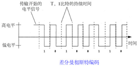
差分曼徹斯特編碼:
在訊號位開始時不改變訊號極性,表示輯"1"
在訊號位開始時改變訊號極性,表示邏輯"0" ;
【注意】:如果在最初訊號的時候,即第一個訊號時:
如果中間位電平從低到高,則表示0;如果中間位電平從高到低,則表示1;
後面的(從第二個開始)就看每個訊號位開始時有沒有跳變來決定:
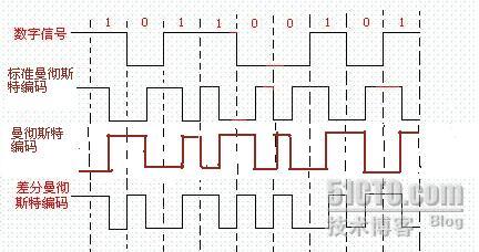

Biphase Mark Coding
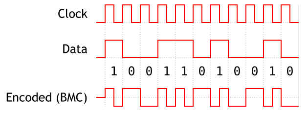
差分曼徹斯特編碼與曼徹斯特編碼的比較
他們的特徵是在傳輸的每一位資訊中都帶有位同步時鐘,因此一次傳輸可以允許有很長的資料位。
- Modulation rate twice that of NRZ and bandwidth correspondingly greater. (Modulation is the rate at which signal level is changed).
- Because there is predictable transition during each bit time,the receiver can synchronize on that transition i.e. clock is extracted from the signal itself.
- Since there can be transition at the beginning as well as in the middle of the bit interval the clock operates at twice the data transfer rate.
- Biphase-manchester: Transition from high to low in middle of interval = 1 and Transition from low to high in middle of interval = 0
- Differential-manchester: Always a transition in middle of interval. No transition at beginning of interval=1 and Transition at beginning of interval = 0